The Absurdly Complex Register Scheme in the Intel 80386
A deep dive into the silicon-level implementation of Intel 80386 registers, revealing six different circuit designs used for 30 physical registers, driven by backward compatibility with 1971-era processors.
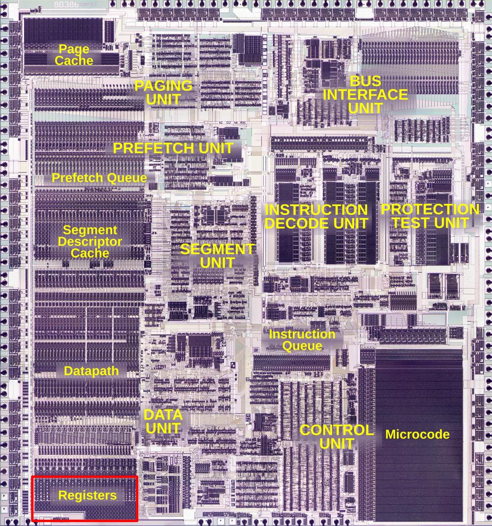
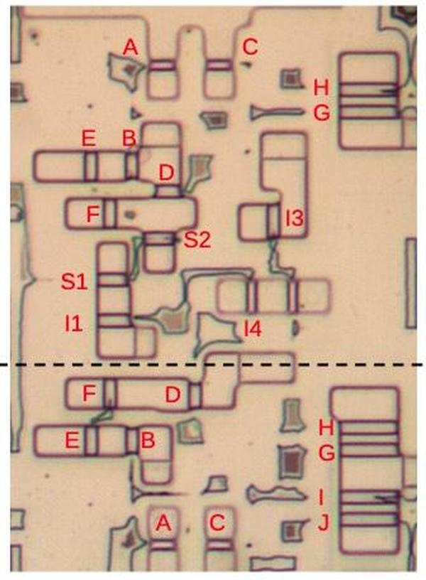
The article begins with an examination of the i386 die under magnification, identifying the register block in the lower-left section. The Intel 80386 (1985) was the first 32-bit x86 processor, containing registers essential for high-speed data processing compared to main memory.
i386 Registers
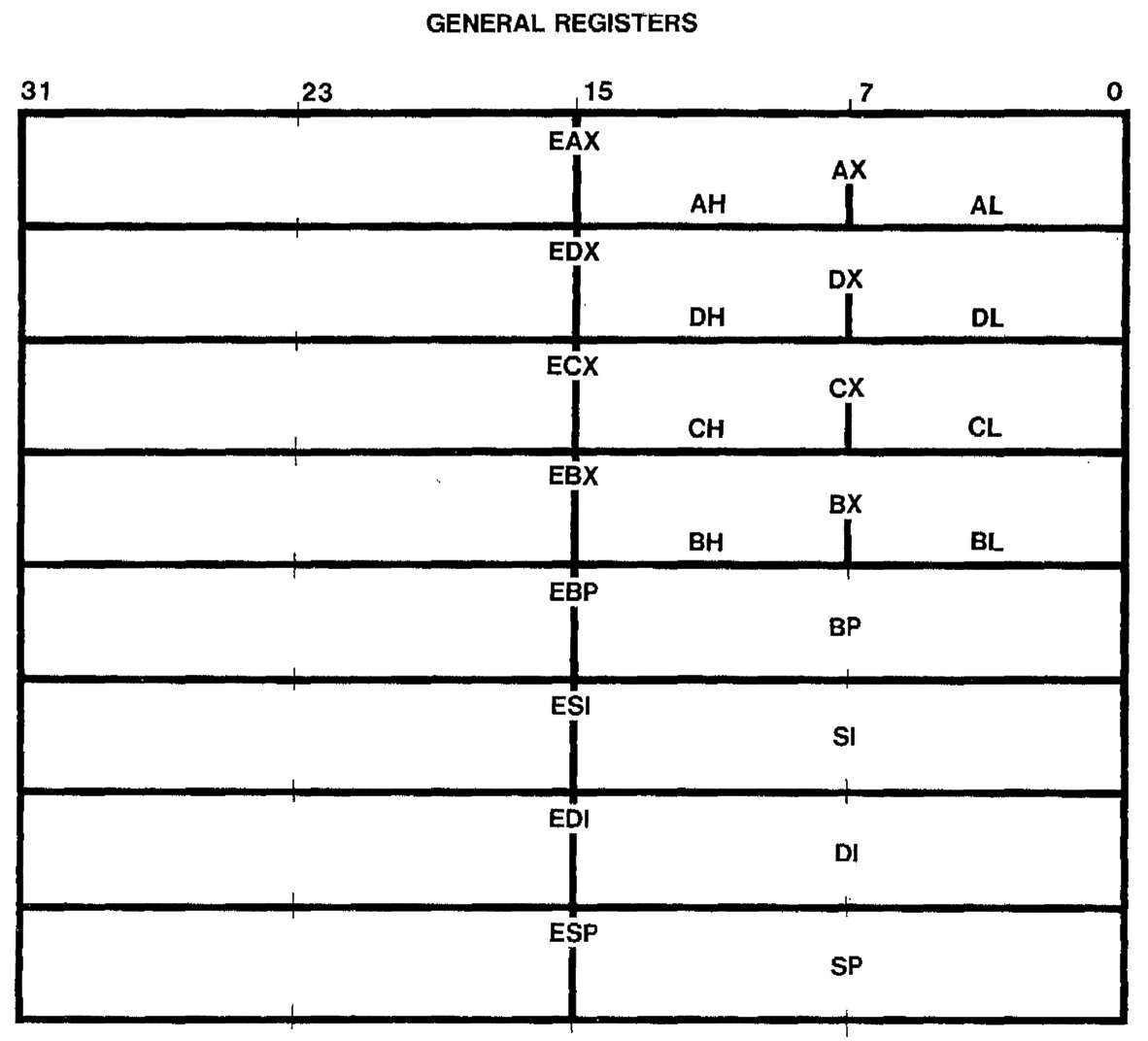
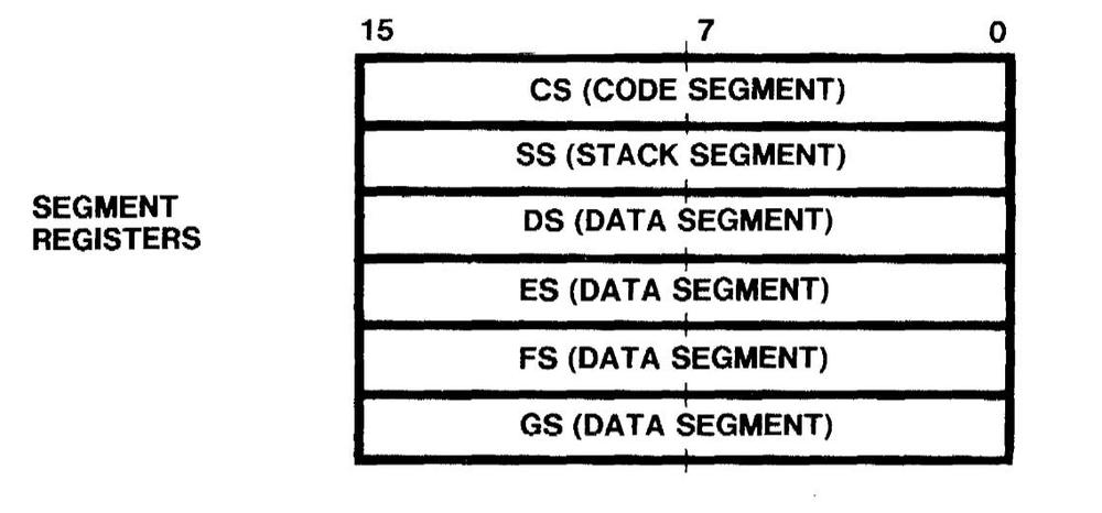
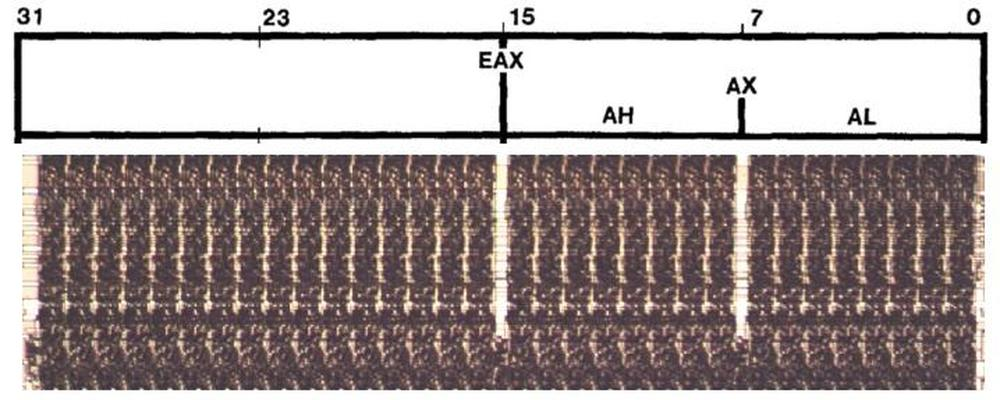
The processor contains 16 registers for application programming. The eight general-purpose 32-bit registers include EAX, EBX, ECX, and EDX. These support backward compatibility through multiple access modes: they can be accessed as 32-bit (EAX), 16-bit (AX), or 8-bit (AL, AH) registers.
Additional registers: EBP, ESI, EDI, and ESP function as 32-bit or 16-bit registers. The processor also includes six 16-bit segment registers defining memory segment boundaries.
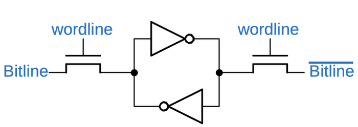
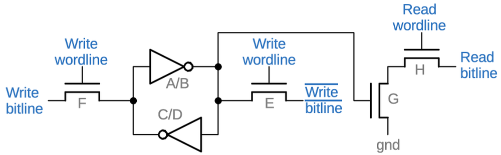
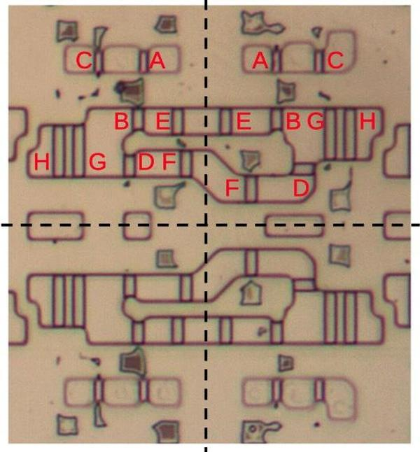
6T and 8T Static RAM Cells
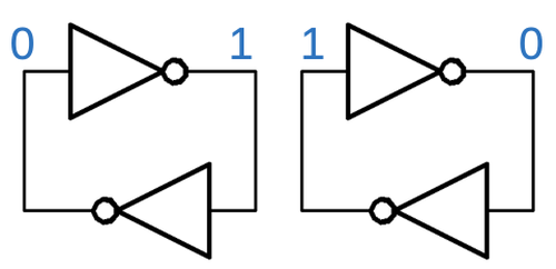
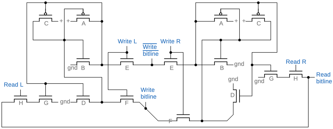
Registers use static RAM cells capable of storing single bits. The implementation uses two logic inverters connected in a feedback loop.
6T Cell Design: Contains six transistors total — two for each inverter plus two pass-through transistors for access control. Reading and writing share the same bit lines, preventing simultaneous operations.
8T Cell Enhancement: Adds two transistors for independent read capability, enabling dual-port operation — one register can be read while another is written.
Pass-through transistors are controlled by a word line, regulating access to storage locations.
Six Register Schemes in the i386
Instead of a single unified design, Intel implemented six different register circuit designs for 30 physical registers. Each is optimized for specific requirements: some cells are combined to double storage density, others support data access in 8, 16, or 32-bit widths.
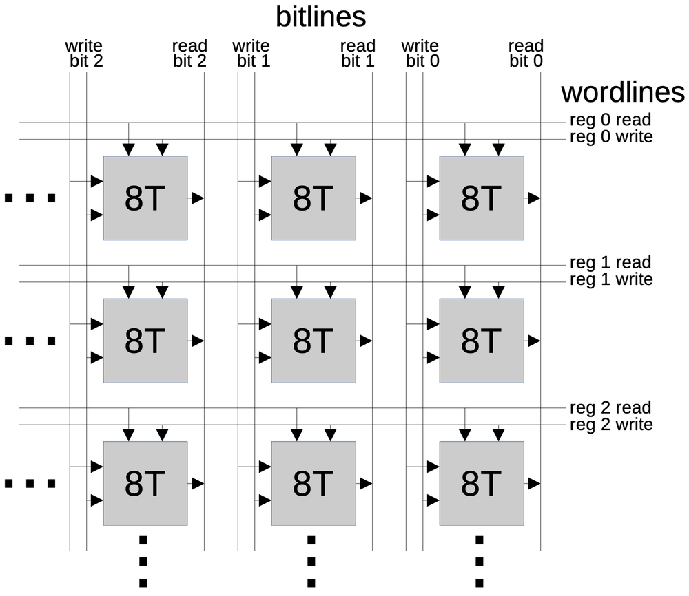
Type (f) — 16-bit Registers (8 total): Use 8T architecture for dual-port capability. Implement double-density layout: two registers per row with interleaved bits, achieving twice the density of other schemes.
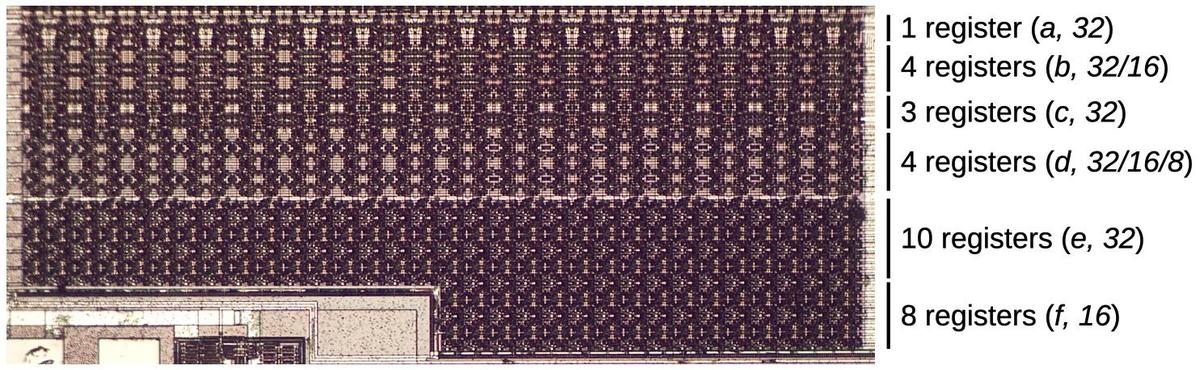
Type (e) — 32-bit Temporary Registers (10 total): Built with 8T cells. Span the full data path width. Support dual-density implementation.
Type (d) — Three-Port General-Purpose Registers (4 total): Use 10-transistor (10T) cells. Enable simultaneous two-register reads with one write. Support partial write: three write buses allow independent updates to different parts of the register — the upper 16 bits, the middle 8 bits, and the lower 8 bits.
Type (c) — Control Registers (3 total): 10T architecture without partial write support. Require full 32-bit writes. Three control lines: two for read selection, one for write.
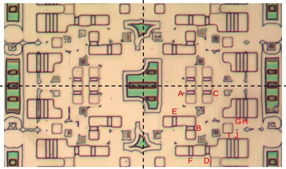
Type (b) — Index Registers (4 total): Support 16-bit and 32-bit writes (not 8-bit). Four control lines total.
Type (a) — Top Register (1 total): Unique capability: can receive a copy of the value in the underlying register. Three control lines: read, write, and copy. Six additional transistors enable direct copying without using read/write buses.
Thoughts on Register Allocation
The mapping analysis suggests:
- Registers EAX, EBX, ECX, EDX → Type (d) registers
- Registers ESP, EBP, ESI, EDI → Type (b) registers
- Segment registers → Type (f) registers
- Control registers CR0, debug registers DR6, DR7 → Type (c) registers
- LOADALL instruction hints at LDT and TR registers among type (f)
The author notes: "I still haven't determined exactly how the i386 registers map to these 30 physical registers" — the precise mapping remains unresolved.
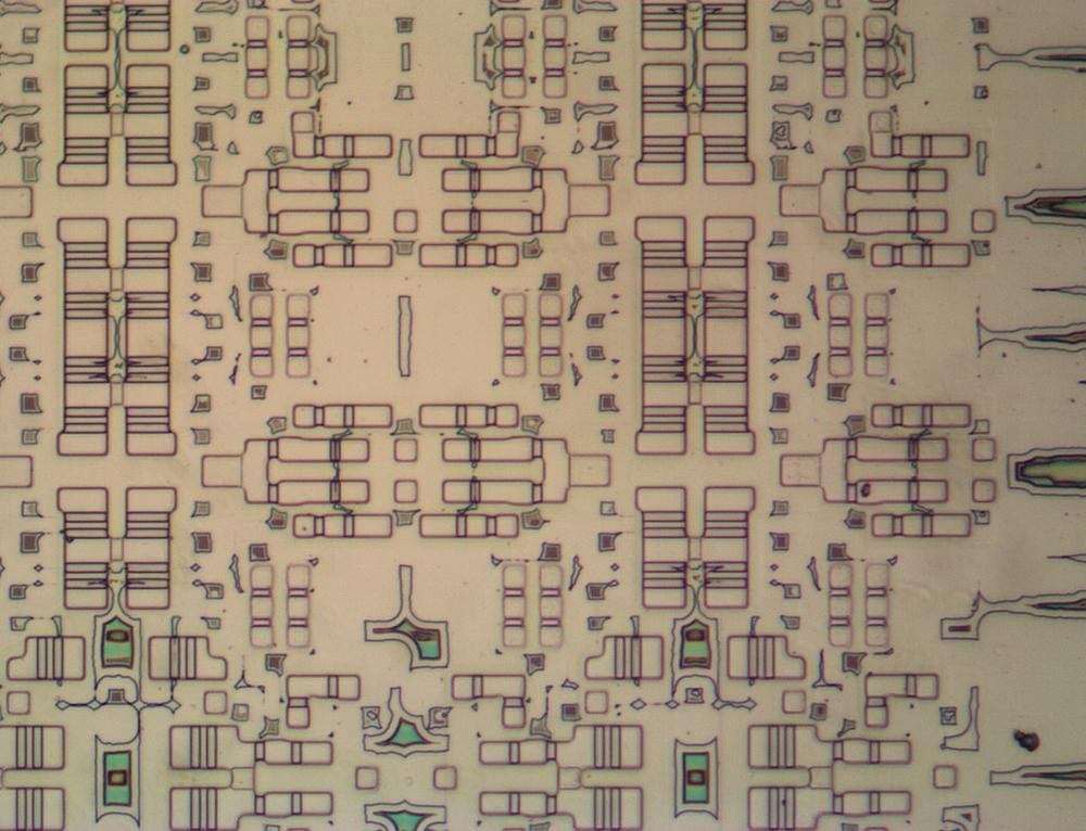
The Shuffle Network
A critical complexity layer addressing the 8-bit access requirement. The problem: an 8-bit ALU operation on register AH requires the bits to be shifted down to positions 7-0.
Solution: Physical bit interleaving in the lower 16 bits. The lower 16 bits of the main registers physically interleave bits from the two low bytes.
Result: AH and AL bits are positioned adjacently, eliminating the need for shifter circuitry. This allows multiplexers to easily select bits from either AH or AL as needed.
The shuffle network sits between the ALU and the register file, reordering bits for storage and retrieval.
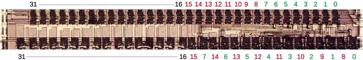
Width Compromise: The shifter circuit measures approximately 54.5 micrometers, versus the standard 60-micrometer cell width. Signal lines require narrowing then widening, creating layout overhead. Intel apparently accepted this trade-off to avoid additional routing space.
Conclusion
Standard processor design textbooks describe simple, uniform register implementations. The i386 reveals that real processors are far more intricate, employing six distinct schemes rather than one.
The register architecture exposes backward compatibility costs. The x86 architecture supports 8-bit register access for compatibility with processors from 1971, requiring additional shuffle networks and interleaved storage.
RISC architectures avoid many such x86 complexities by design.

Notes
Note 1: OS-specific registers (GDTR, LDTR, IDTR, TR, CR0-CR3, DR0-DR7) are located elsewhere on the chip.
Note 2: Write drivers use weak pull-up transistors that enable strong signal overdriving.
Note 3: Pass-through transistors use NMOS-only design.
Note 4: Reads use a bit line precharge mechanism.
Note 5: Buffering is required to prevent cross-cell interference.
Note 6: The flags register and instruction pointer have different implementations across processor generations.
Note 7: Historical context links x86 architecture to the Datapoint 2200 (1971), explaining the origin of dual-register pairs.
Note 8: Comparison with 16-bit 8086 interleaving approaches.
Note 9: ROM is placed beneath the shuffle network, requiring constant bit interleaving.
Note 10: The ALU section has separator logic between bits 7-8 and 15-16.
FAQ
What is this article about in one sentence?
This article explains the core idea in practical terms and focuses on what you can apply in real work.
Who is this article for?
It is written for engineers, technical leaders, and curious readers who want a clear, implementation-focused explanation.
What should I read next?
Use the related articles below to continue with closely connected topics and concrete examples.