RAM: A Comprehensive Guide. Part 1 — The Physical Design of RAM, from Silicon Atoms to Real Chips
A deep-dive into how RAM actually works, starting from the behaviour of individual silicon atoms and ending with the complete architecture of a physical memory module. The article builds every concept from first principles — semiconductors, transistors, capacitors, memory cells — before showing how they are assembled into the chips and DIMMs on your motherboard.
Editor's Context
This article is an English adaptation with additional editorial framing for an international audience.
- Terminology and structure were localized for clarity.
- Examples were rewritten for practical readability.
- Technical claims were preserved with source attribution.
Source: the original publication
Introduction: What This Article Covers and Why There Are Two Parts
Originally, I didn't want to split this article into parts — I wanted to fit everything into one: from atoms and transistors to the segmented memory model in x86_64 and virtual memory pages in Linux. But had I done that, the reading time indicator would have exceeded an hour and the material would have been too scattered. So I decided to split the comprehensive description of RAM into two parts: the physical design of RAM and the logical design of RAM.
Across two articles, the first of which you are reading right now, we will walk through every level of understanding, starting from the atomic model taught in 8th-9th grade physics all the way to virtual memory in modern operating systems (specifically Linux).
Special attention in this article, since we are examining physical aspects, will be given to the transistor (and the capacitor), the most important circuit element that, without exaggeration, underpins all of modern microelectronics.
Simply saying that a transistor works like an electrical switch, passing or blocking charge, would be like saying that RAM can simply read and write information at a specific address. So we will try to understand its nature and operating principles in every detail, gradually increasing complexity: from the atom to the RAM stick.
It's also important to note that there are two main types of RAM: DRAM and SRAM. In this article, we are examining DRAM specifically, which I kindly refer to simply as RAM to avoid unnecessary confusion. SRAM works somewhat differently, using flip-flops, and is used as CPU cache memory (but that's a whole different story...)
IMPORTANT!!! This article does not claim to provide strict formal physics definitions, as it was written by someone who is far from being a physicist. The goal of this analysis is to build context in the subject and understand the idea as a whole — to construct an abstract model of what happens inside a PC case. This is perfect for those who are completely unfamiliar with this topic or understand it only vaguely but want to understand it!
The RAM Cell: Transistor and Capacitor
A RAM cell is much simpler and more understandable than a solid-state drive (SSD) cell. While a clear understanding of SSD operating principles requires knowledge of quantum physics (specifically the tunneling effect), understanding RAM only requires remembering a couple of things from high school physics. The general workings of an SSD were covered in my previous article.
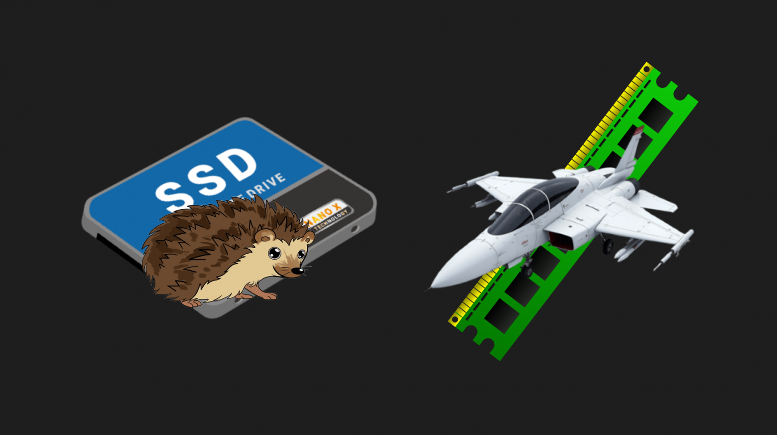
Moreover, accessing an SSD memory cell (read/write) takes about 50 microseconds, whereas accessing a RAM cell takes 17 nanoseconds — more than 3,000 times faster.
For comparison, a supersonic fighter jet flying at Mach 3 (three times the speed of sound) is roughly 3,000 times faster than a hedgehog. That's the colossal difference between the speed of memory access in SSD versus RAM:
That's why reliable SSDs are used for long-term storage — they don't require constant uninterrupted electrical power unlike RAM (more on volatility later) — while fast RAM is used for data of currently running programs. Loading any "heavy" game, like GTA 5, is nothing more than copying all the textures and game data from the SSD into RAM for fast access during gameplay. If the data forming the game process were directly read from and modified on the SSD, the game would turn not into a movie, but into a set of slowly changing static frames.
A RAM cell consists of two basic circuit elements: a transistor and a capacitor. Even if you never liked or understood physics, that's okay — we'll break down these two fundamental elements of all modern electronics literally on our fingers and try to make it not boring, quick, yet with complete understanding.
So let's take a deep breath and begin — our task is to understand how the transistor works and how RAM works overall!
What Are Conductors, Semiconductors, and Insulators?
When talking about physics, it's worth sticking to a specific model that adequately reflects the processes occurring in the objective world. Below we will talk about atoms and types of substances: conductors, insulators, and semiconductors. There are quite a few models of atomic representation — from the most primitive and outdated ones proposed a couple of centuries ago, to the most revolutionary quantum physics models where the electron is considered not as a "ball" (or a specific point in space) but as some probabilistic structure. But let's not go there — I am absolutely not a specialist in quantum physics :)
And this doesn't mean that different models completely contradict each other — they simply reflect either different aspects of the modeled object (in our case, the atom), or they bring us closer or further from what actually happens in the world around us.
We will stick to the atomic model proposed by Rutherford in 1911 (the Planetary Model of the Atom) with small refinements from Niels Bohr in 1913 (the Bohr Model of the Atom). And yes, these models will fully suffice for us, just as they sufficed for people in the early 1910s, when airplanes and airships were already flying through the sky, and the world knew of quite a few electromechanical machines (for example).
The Planetary Model of the Atom
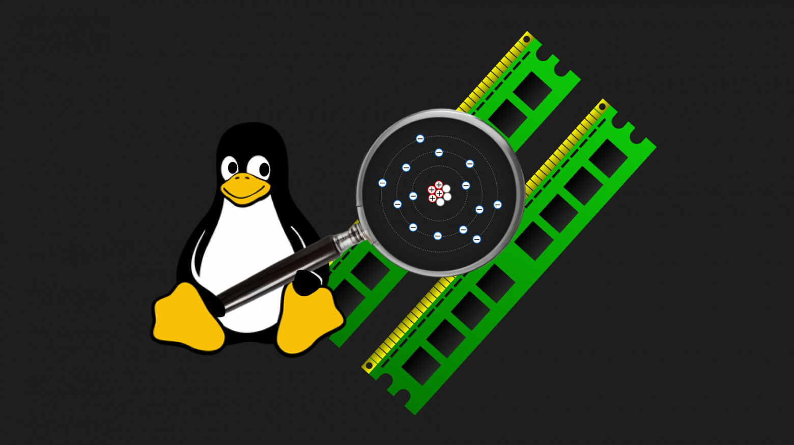
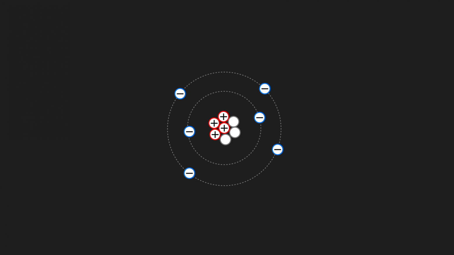
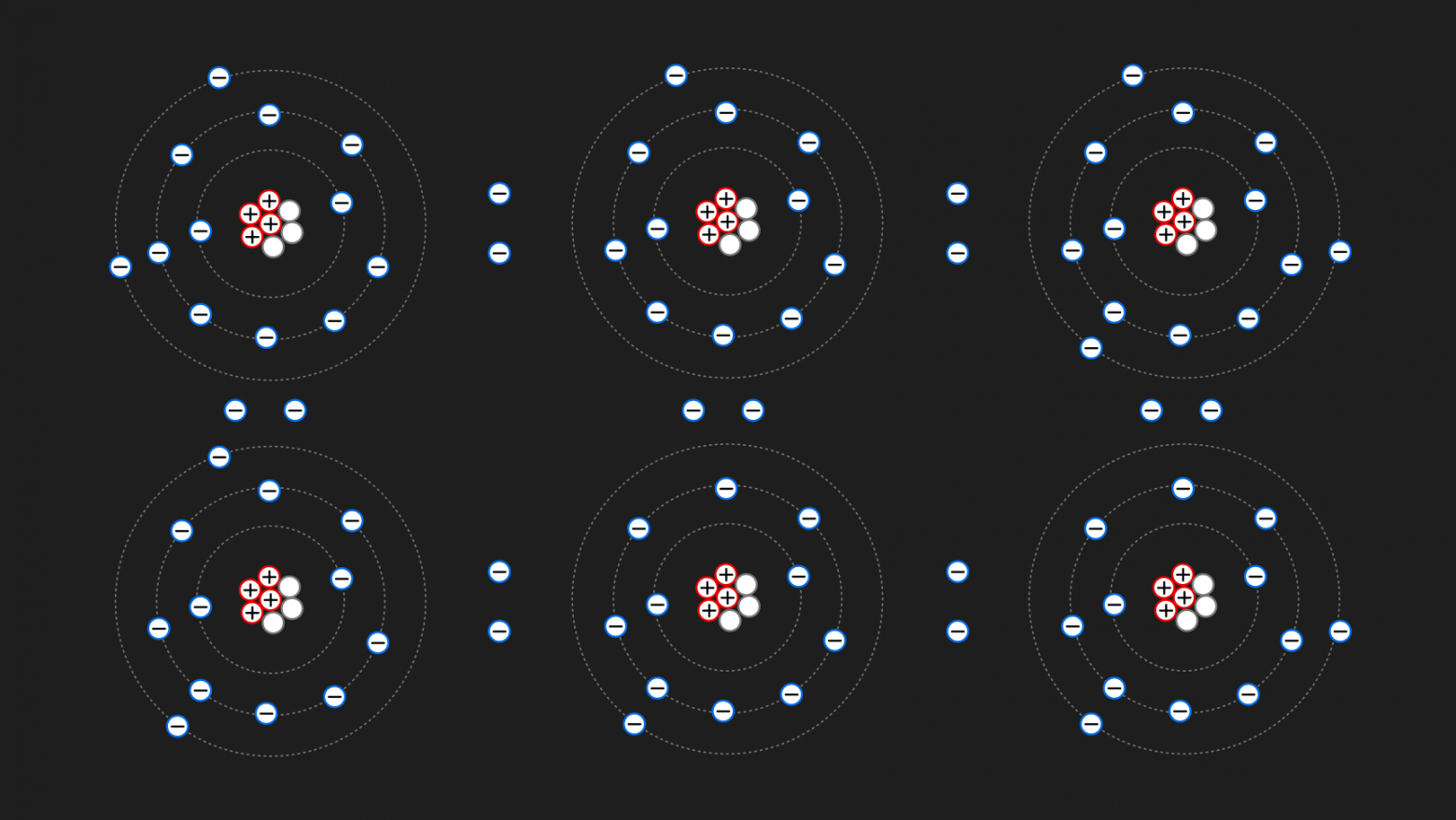
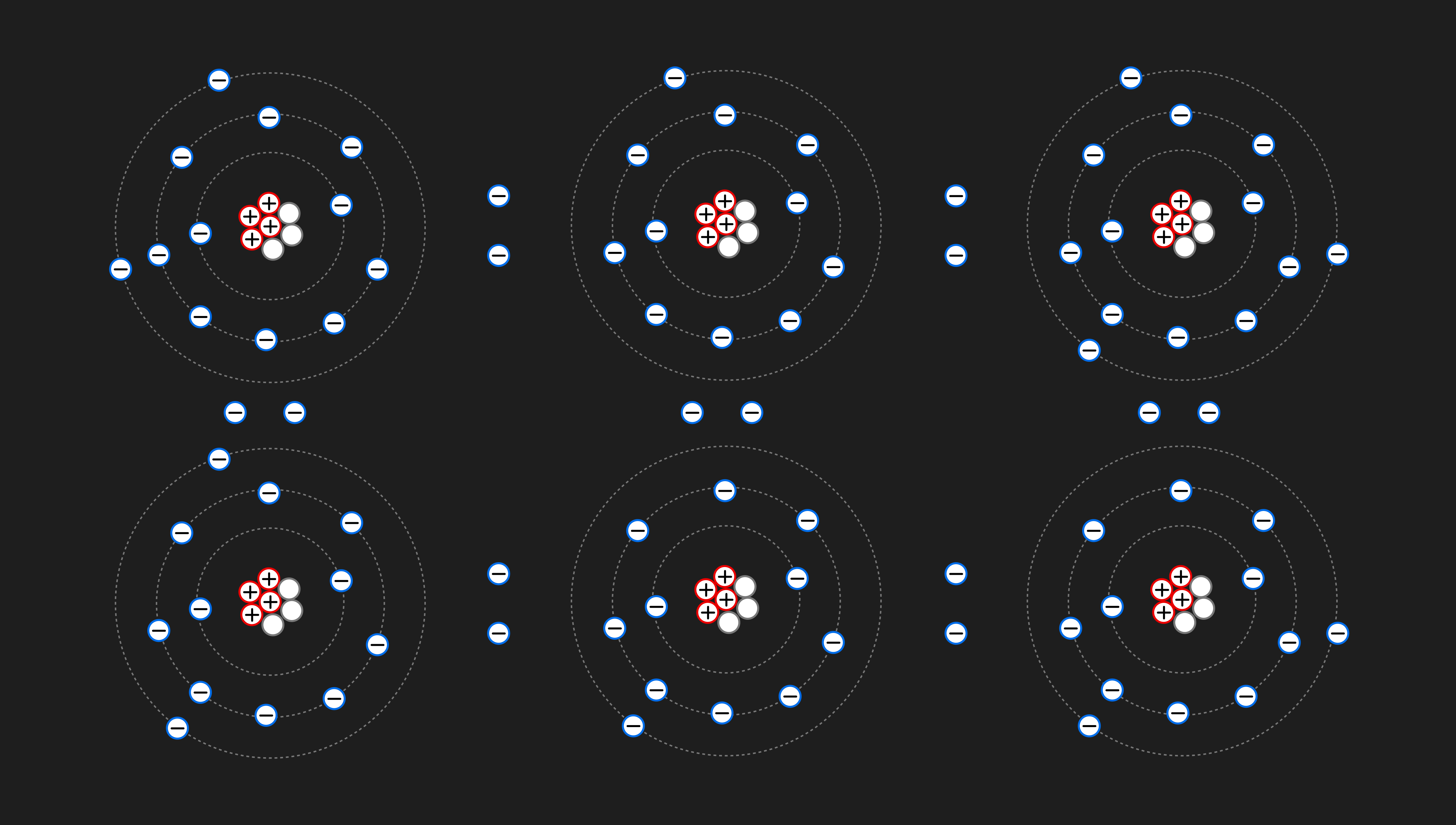
Meet the Silicon atom:
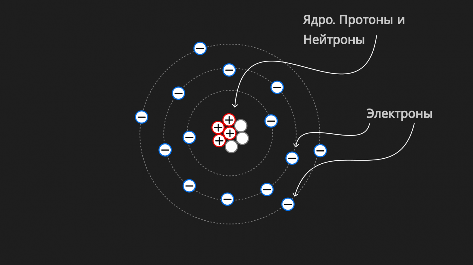
The planetary model of the atom describes it as follows: "The atom consists of a tiny positively charged nucleus, in which almost all the mass of the atom is concentrated, around which electrons orbit — similar to how planets move around the Sun."
The nucleus consists of protons (positively charged particles) and neutrons (particles with no charge). Electrons are negatively charged.
We said that the nucleus is positively charged and electrons are negatively charged. But what are these "plus" and "minus"? In fact, it's simply a convention introduced long ago by Benjamin Franklin (the same one depicted on $100 bills). You could name them the other way around — physics wouldn't change because of it.
What matters is not the sign (the name), but how charges interact:
- Charges of opposite sign attract;
- Charges of the same sign repel.
That is, some attract and some repel — they were divided into two conventional groups called "plus" and "minus," that's it! We, like all of physics, cannot answer the question WHY this is so (i.e., why charges behave this way and why atoms and molecules are the way they are). We can at best approximate an answer to the question HOW this is so (i.e., how charges behave and how atoms and molecules are structured).
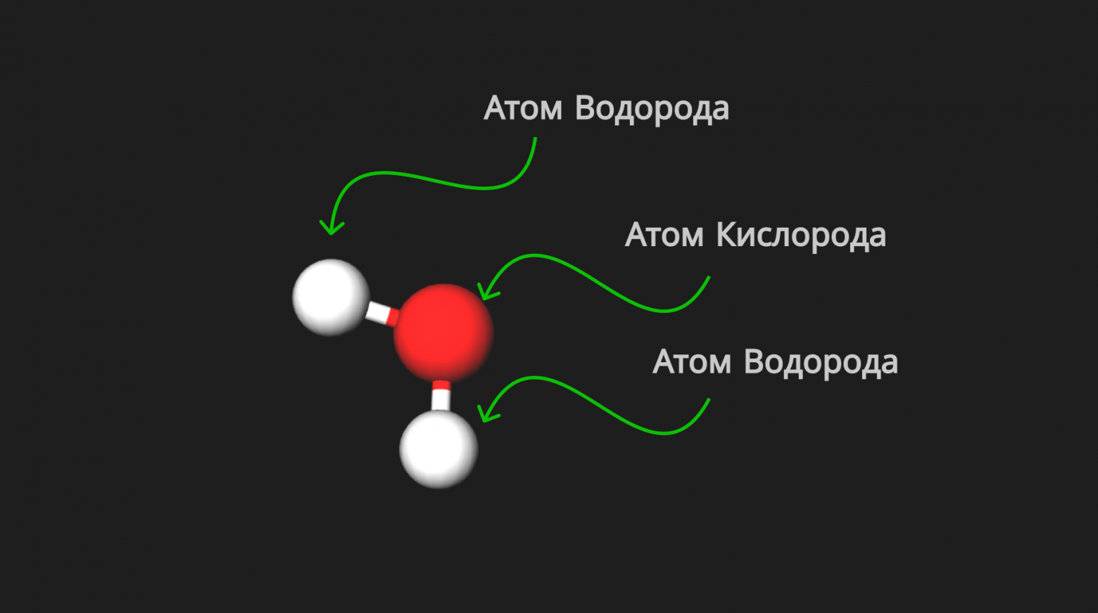
How? Very simply (just kidding). Substances consist of molecules, which in turn consist of atoms. Atoms consist of a positively charged nucleus and negatively charged electrons (picture above). Different configurations of atoms give rise to different molecules. For example, the well-known formula for a water molecule H₂O, which consists of two hydrogen atoms (H₂) and one oxygen atom (O):
Based on the model we've adopted, electrons in an atom exist at different "orbits." Why different ones? Because some electrons have more energy and some have less. The more energy they have, the more strongly the negatively charged electrons can resist the attractive force of the positively charged nucleus (since charges of opposite signs attract), and the "higher" orbits they occupy. It follows inversely that the less energy an electron has, the closer it is to the nucleus.
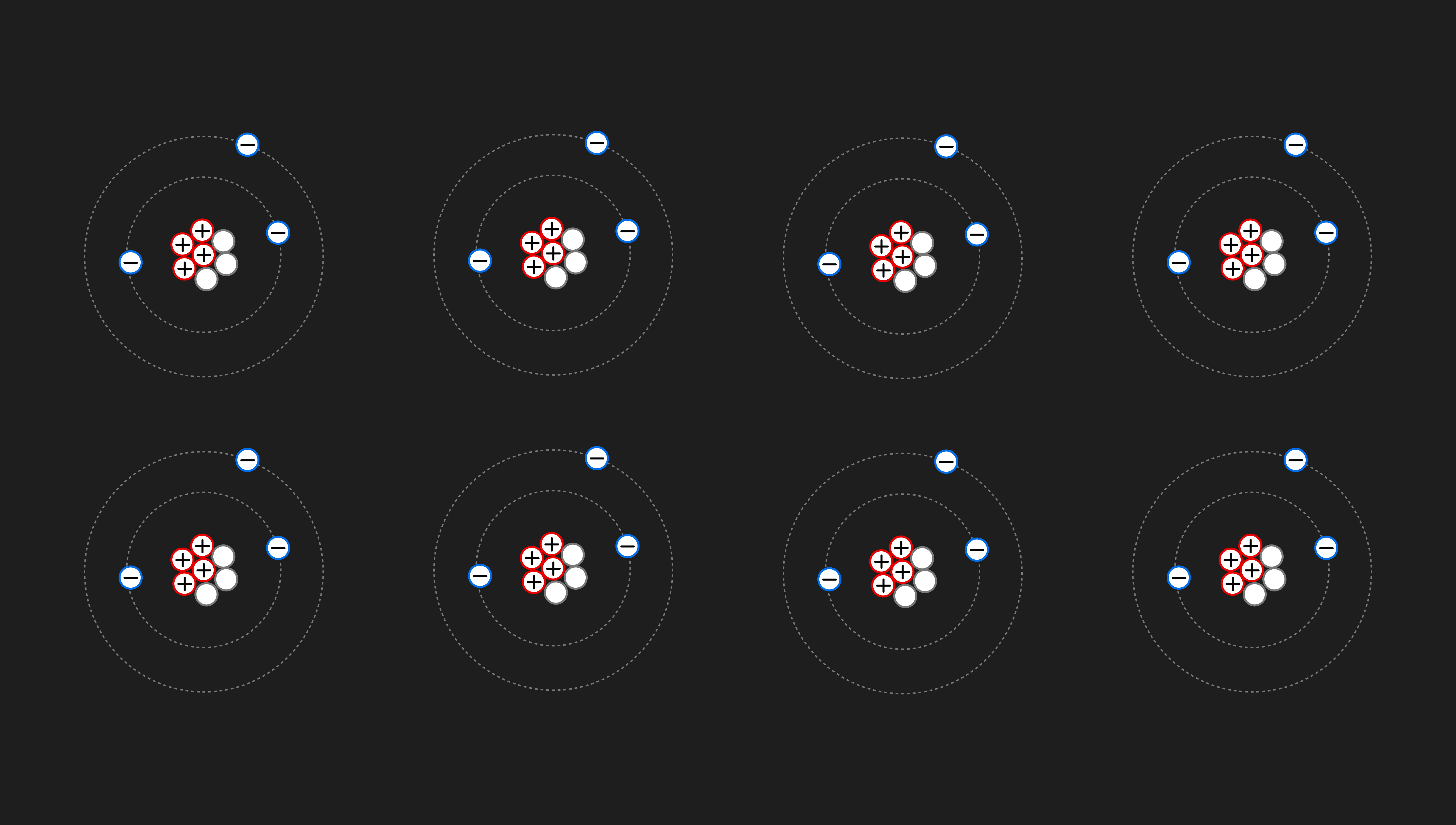
Excellent — so what differentiates the Silicon atom in the picture above from, say, a Carbon or Helium atom? Of course! They differ from each other only in the number of electrons at different "orbits"/levels and, naturally, the number of those levels themselves (and the number of neutrons and protons in the nucleus, but that's not so important for us right now).
Here's the Carbon atom:
The Carbon atom has 2 electrons on the first orbit and 4 electrons on the second; there are only two orbits.
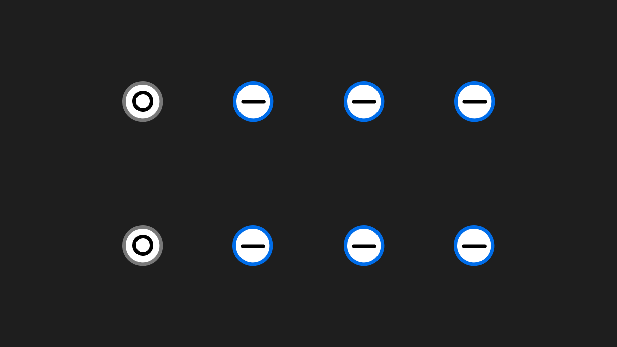
And here's the Helium atom:

The Helium atom has 2 electrons on its first and only orbit.
Yes, these electron configurations (and protons with neutrons in the nucleus) are all that differentiates atoms from each other, and it is solely thanks to these differences that a colossal variety of molecules are born (since different atom configurations give rise to different molecules — we looked at H₂O above), the tangible material things we perceive, and the entire world around us!
Outer/Valence Electrons
I think many people are familiar with the word "Valence" from school. Yes, it scared me too, but in reality there's nothing frightening about it.
The word "valence" comes from the Latin "valentia," meaning "strength," "power," or "capability."
Outer/Valence electrons are those electrons that are on the outermost level (the last orbit — see pictures above) of an atom. Valence electrons, translated literally, are "capable electrons" — electrons capable of interacting with other atoms.

Since they are the farthest from the nucleus and least constrained by its attractive force (since the electron is "−" and the nucleus is "+", and "+" and "−" attract), they can occasionally "jump" to other atoms (we'll see how shortly) — that is, they are literally "capable" of this! Or, as we said earlier, the more energy an electron has, the farther it is from the nucleus, since through this energy it can resist the nucleus's attractive force. Therefore it can be called a "Strong electron," which is also a literal translation of the expression "Valence electron" :)
Now we will examine this idea in detail using conductors, insulators, and semiconductors.
Conductors
In conductors, the outer/valence electrons are very weakly bound to their atoms. So weakly that the strength of their interaction with their own atomic nuclei is comparable to the strength of interaction with the nuclei of neighboring atoms. As a result, electrons transition into a free state and can move through the conductor. This is especially characteristic of metals.
Let's look at a piece of Lithium (Li):
As we can see, the electrons from the outer orbit are so weakly attracted to their own atoms' nuclei that they constantly "migrate" to other atoms, traveling through the conductor. Such wandering valence electrons are called free electrons or conduction electrons.
Under the influence of an external electric field, free electrons begin to move in a directed manner, which is what we call electric current or the flow of electric current!
What is an external electric field? That's a topic for a separate article with a substantial introduction about how to perceive the word "field" — here's a good video on this topic. In our case, we can say the following:
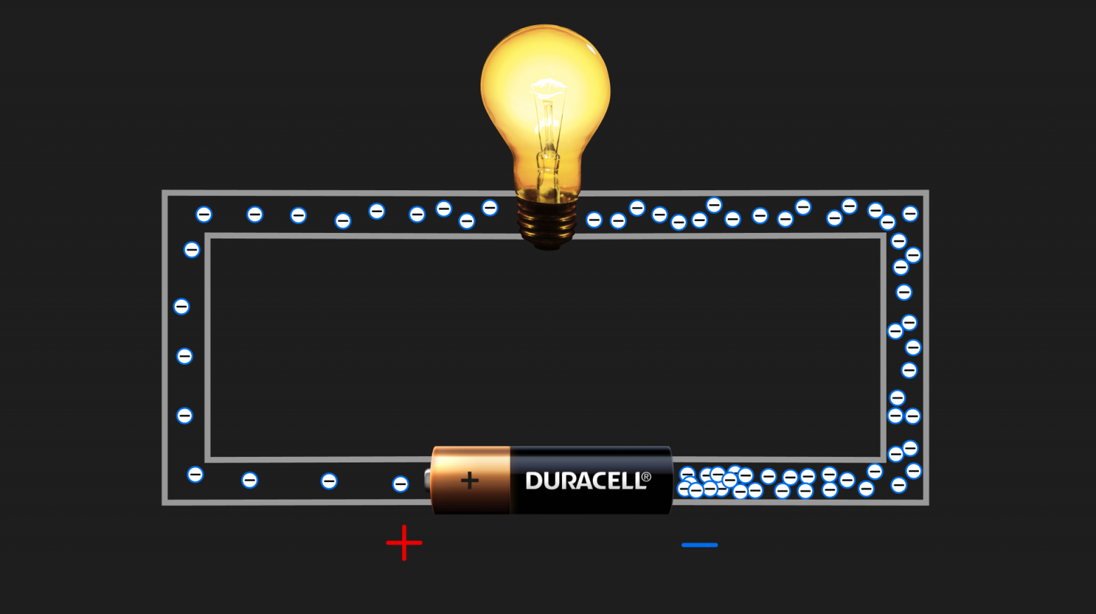
Here's the simplest circuit consisting of a battery and a lightbulb connected by a wire made of some conductor. The battery, through chemical reactions inside it (this can and should be skipped for now), creates an excess of electrons at the negative end and a deficit at the positive end. In other words, it works like a pump, sucking electrons from the positive end to the negative end, which is clearly visible in the picture. The battery doesn't create new electrons — it only moves existing electrons from one pole to the other.
The electrons shown in the picture above are precisely those free electrons. They travel through the conductor (the wire). The battery created an electric field (don't be afraid of this term), which forced the free electrons to move not chaotically but in an orderly fashion — from "−" to "+" of the battery. From the area of excess to the area of deficit. In other words, an electric field is a certain "thing" that arises when the harmony of charges is disturbed (one end has excess electrons, the other has a deficit) and it wants to restore that harmony (which is why current flows). Such a balance, maintained by the laws of the universe :)
To summarize: Conductors are substances capable of easily conducting electric current under the influence of an electric field (in our example, the battery generated the field) through free electrons.
Insulators (Dielectrics)
In insulators, everything is quite different. Electrons are rigidly bound to their atoms. There are no free electrons in insulators, and consequently they do not conduct current.
Let's look at a piece of Helium (He):
That is, the valence electrons in insulators don't have enough energy to become free. Yes, under a colossally strong field, dielectric breakdown can occur, but that's a separate topic. The link is only for the very curious :)
Semiconductors
As the name suggests, semiconductors occupy an intermediate position between conductors and insulators.
Semiconductors are similar to insulators in that normally all their valence electrons are in bound states. Electrons of neighboring atoms are attracted to each other in pairs (electrons are jointly held by two nuclei of neighboring atoms). This bond is called covalent. The Latin prefix "co" means joint/shared, and "valent" we've already analyzed. So a covalent bond is a "jointly strong" bond. I think you get it :)
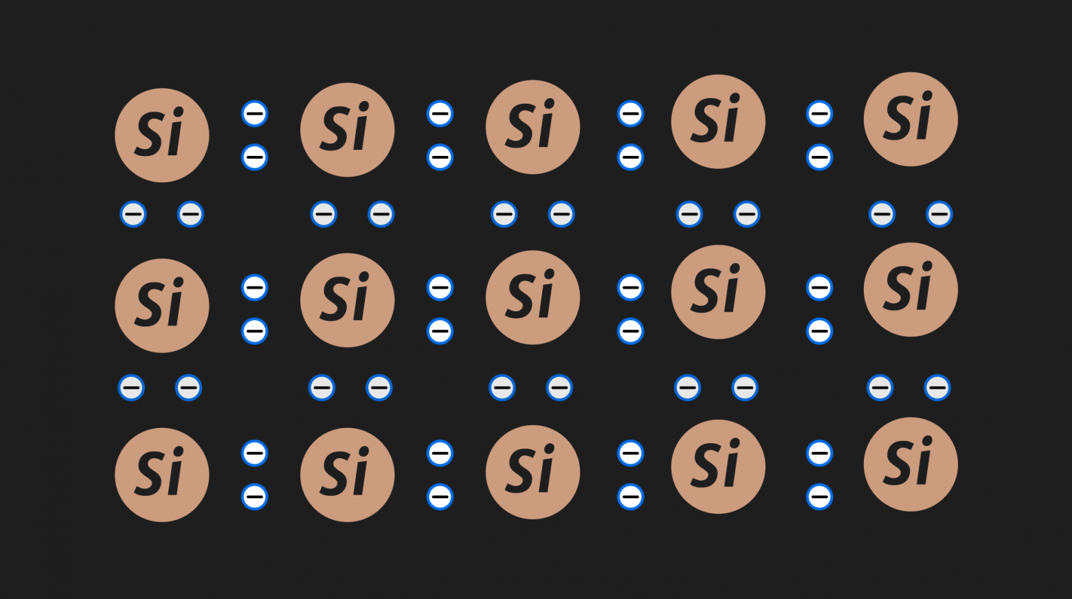
Going forward, we will look at Silicon, since it currently lies at the foundation of all semiconductor technologies due to certain properties such as its melting point or availability (i.e., easy to extract). For us right now, it's not very important why Silicon specifically — let's just accept it as a fact.
Silicon has 4 electrons on its outer/valence level; it gives one to form a bond with each of its neighboring atoms.
Let's look at a piece of perfectly pure (this only happens in pictures) silicon (the nucleus and non-valence electrons will be denoted simply as a circle with the element name):
Look at the electrons on the outer levels in the picture and try to mentally expand the picture. For example, the top-center atom gave one electron to bond with its left neighbor, another to bond with the right one, and a third to bond with the one below. If we drew another row of atoms above, the last electron would also go to bond with the upper neighbor. And so on for every atom. I think the idea is clear.
But the outer electrons in semiconductors are bound to their atoms more weakly than in insulators and can occasionally break free from their atoms (as happens in conductors) and become free electrons. Electrons are especially likely to "break free" when the semiconductor is heated or when an external voltage is applied to it (we'll need the second one later).
Let's heat a piece of Silicon (Si):
In the place where an electron "broke free," a so-called hole is formed. A hole is not a particle — it is the absence of a particle. Notice in the animation above: in the places where electrons left their position, gray imaginary particles with a circle in the center appear — that's how I drew a hole. Physicists simply decided to denote the absence of an electron where it "should be" as a "hole."
A hole is — attention, very scary word — a quasiparticle! The word "quasiparticle" comes from the Latin "quasi" meaning "like" or "sort of," and the word "particle."
That is, a hole is "sort of" a particle. The absence of an electron can be treated "like" a particle because another electron can move into this vacant spot, thereby closing the hole but forming a new one in the place it "jumped" from. I recommend looking carefully at the animation above and understanding it visually. A hole is nothing more than a convenient model for the absence of an electron; in calculations, it is treated as a quasiparticle with a positive charge.
And here's why the region of space (hole) where an electron is absent in a semiconductor was given its own name:
Look and answer the question: "Are the electrons moving left, or are the holes moving right?" What nonsense! Of course the electrons are moving left — the electron is a particle (which even has mass) and it is what carries the charge, while a hole is simply the absence of a particle! But! Formally, you can say that the holes are moving right — mathematical calculations don't care what is a particle and what is not. What matters is the mathematical model!
But what makes semiconductors so interesting, and why do we need all this?
- They're interesting because their conductivity can be easily controlled, which cannot be said of regular conductors or insulators. That's why they've proven themselves so well in microelectronics (logic circuits), where it's necessary to clearly track the state of all components and have the ability to change it;
- And we need this to understand the most important element in any modern system — from smart (or not so smart) kettles to cloud clusters and supercomputers. This element is the transistor!
Types of Semiconductors and the p-n Junction
In the section above, we looked at pure semiconductors — semiconductors without impurities. Roughly speaking, if we call a piece of material a piece of silicon, it means that at the atomic level, this piece contains only silicon atoms; atoms of no other substance are mixed into it.
Of course, achieving absolute 100% purity of a semiconductor is impossible, but extremely pure materials can be obtained under laboratory conditions.
But we can deliberately "contaminate" a semiconductor with impurities (atoms with a different number of valence electrons) to increase the number of free electrons or holes in the semiconductor!
Let's look at a piece of perfectly pure silicon (the nucleus and non-valence electrons are shown simply as a circle with the element name):
N-type Semiconductor
For example, we can add atoms of Phosphorus — silicon's neighbor in the periodic table — which has 5 valence electrons, to silicon which has 4:
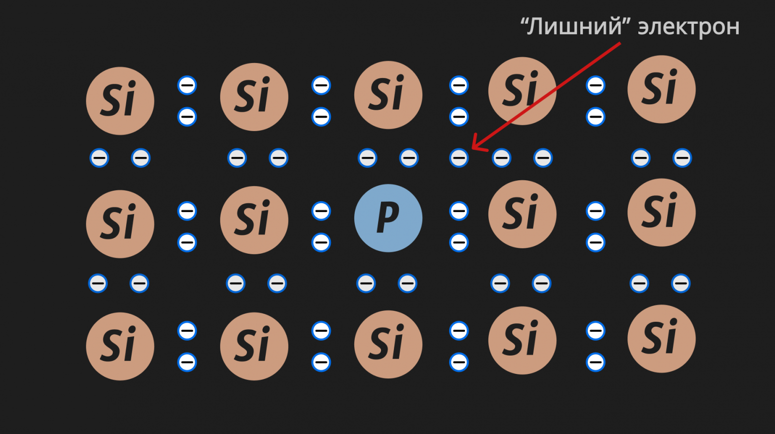
Four of phosphorus's electrons form bonds with neighboring silicon atoms, while the 5th turns out to be "extra." Such extra electrons easily leave their parent atoms, increasing the number of free electrons (conduction electrons) and the overall conductivity of the semiconductor.
So in such a semiconductor, there are more free electrons than holes. Such semiconductors are N-type semiconductors. "N" stands for negative, since the electron has a negative charge and their number predominates in an N-type semiconductor!
P-type Semiconductor
You can do the opposite — "contaminate" the semiconductor with atoms that have fewer valence electrons. For example, for our silicon with 4 valence electrons, we use Boron atoms with 3 valence electrons:
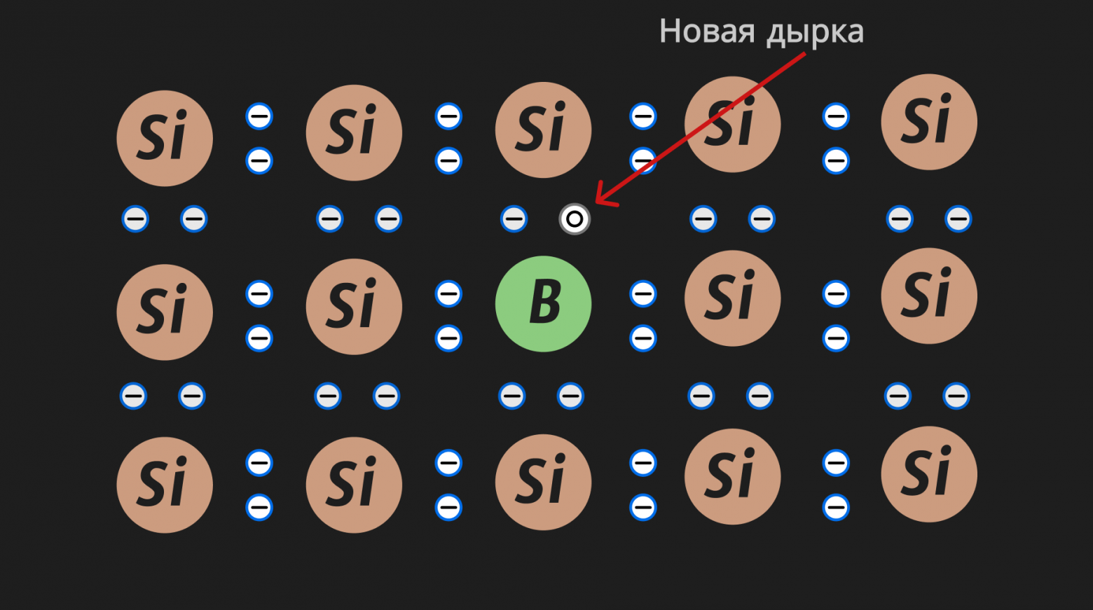
Such semiconductors are called P-type semiconductors. "P" stands for positive. I think it's already clear why :) Because in P-type semiconductors, holes predominate, and the absence of a minus is perceived as a plus. A hole is a quasiparticle with a positive charge, as we discussed above.
This also leads to enhanced conductivity of the semiconductor. That is, in any case, conductivity is caused by electrons "wandering" through the semiconductor, but in the case of N-type, electrons simply "travel" through the material like free electrons in regular conductors, while in the case of P-type, electrons "travel"/"jump" from hole to hole. But to avoid confusion and clearly understand the type of semiconductor, we say that the holes move (again, for convenience and transparent calculations on paper).
Therefore, semiconductors have two types of conductivity: electronic (N-type) and hole (P-type).
The p-n Junction
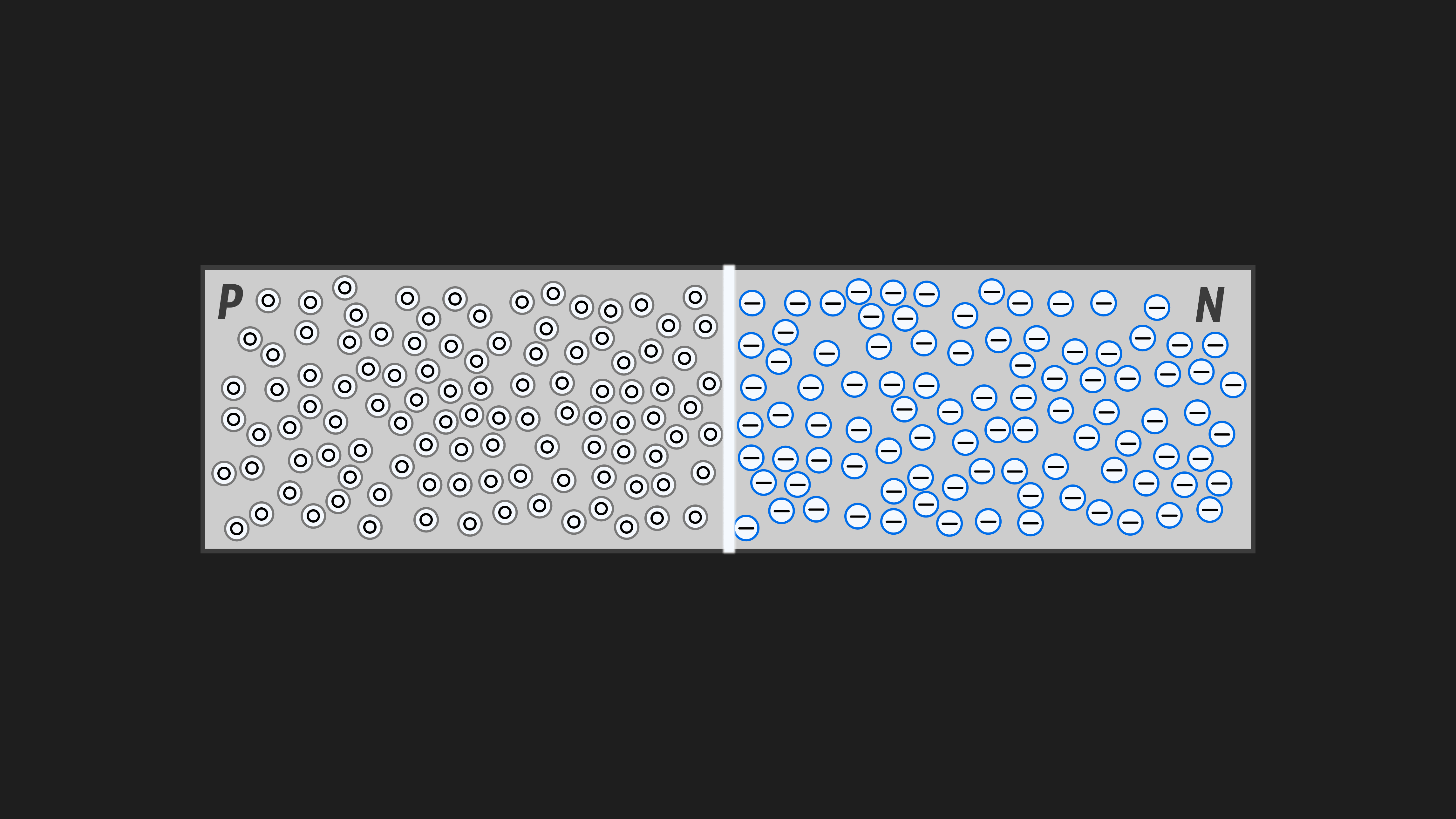
The key idea behind the transistor is the p-n junction. It sounds a bit scary, but in reality, a p-n junction is simply two semiconductors of P and N types joined together. From now on, we will show in our pictures only free electrons and only holes, to avoid cluttering the illustrations with individual atoms and unnecessary details:
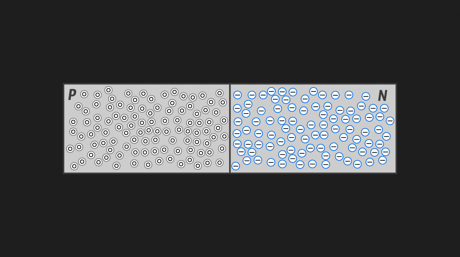
Obviously, some holes from the P-type semiconductor will flow into the N-type semiconductor, and some electrons from the N-type semiconductor will flow into the P-type semiconductor. Yes, holes don't actually flow anywhere — that's the formality we discussed above. Just imagine how electrons from the N-type semiconductor occupy vacant spots (holes) at the boundary with the P-type semiconductor. When electrons from N cross over to the "edge" of P, they leave their position in N — and holes form in their place. Thus, you could say the holes are flowing rather than the electrons — just visually, empirically (see animation below).
And keep in mind that the picture only shows free electrons and holes; we moved away from illustrating individual atoms when we looked at semiconductor types, otherwise the picture would be too cluttered. If you didn't quite understand this idea, I recommend re-reading this section from the beginning.
Thus, at the boundary of the semiconductors, a depletion region forms:
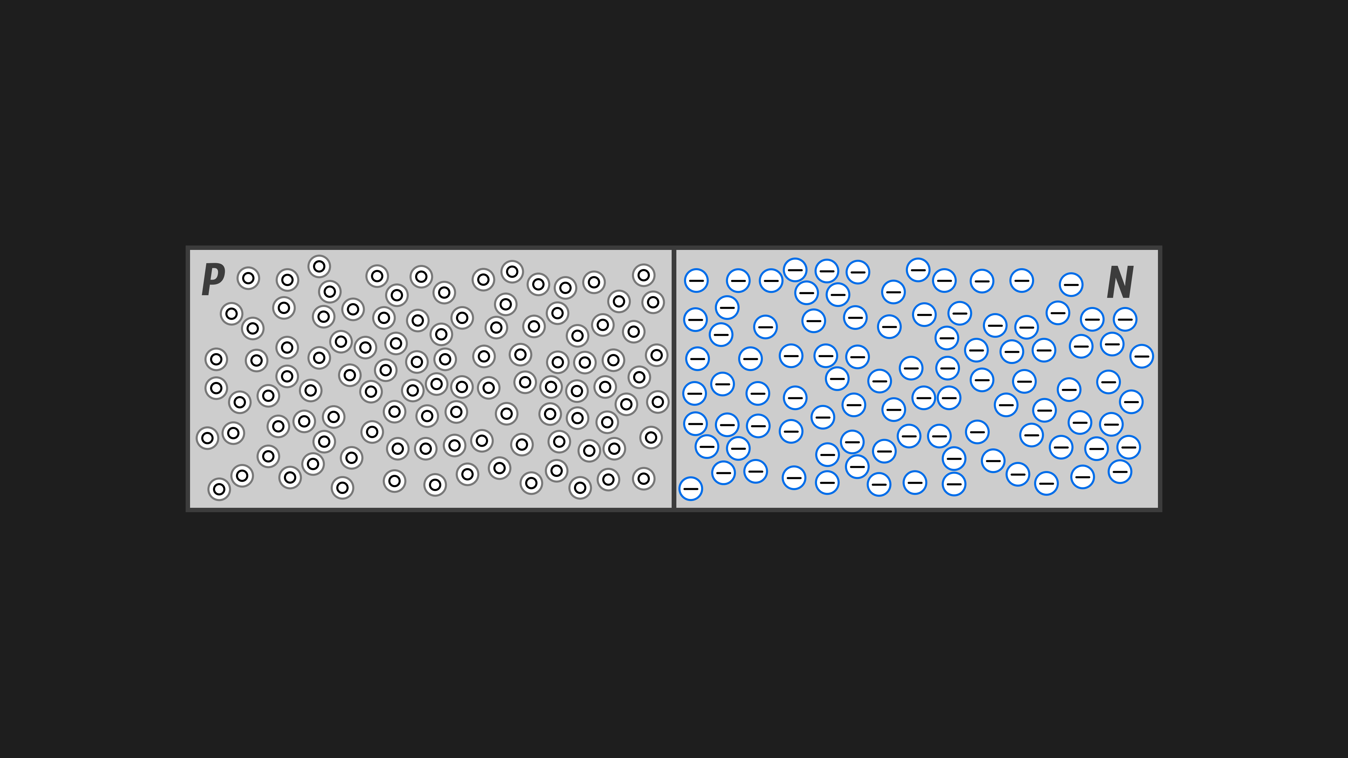
The animation above is not entirely accurate and very simplified, but it is illustrative. Electrons and holes don't simply swap places — they recombine. That is, electrons from N "jump" into these holes at the junction, and in the middle of the two different-type semiconductors, a pure semiconductor forms!
Understand? The left piece has a deficit of electrons, and the right one has an excess. When they are joined, a small region forms at their boundary where the material comes into "harmony." As we already know, a pure semiconductor conducts current poorly, which is why this region, besides being called the depletion region, is also called the barrier region. The barrier region will not conduct current.
Let's denote the expansion of the barrier region this way (the same recombination we discussed above):
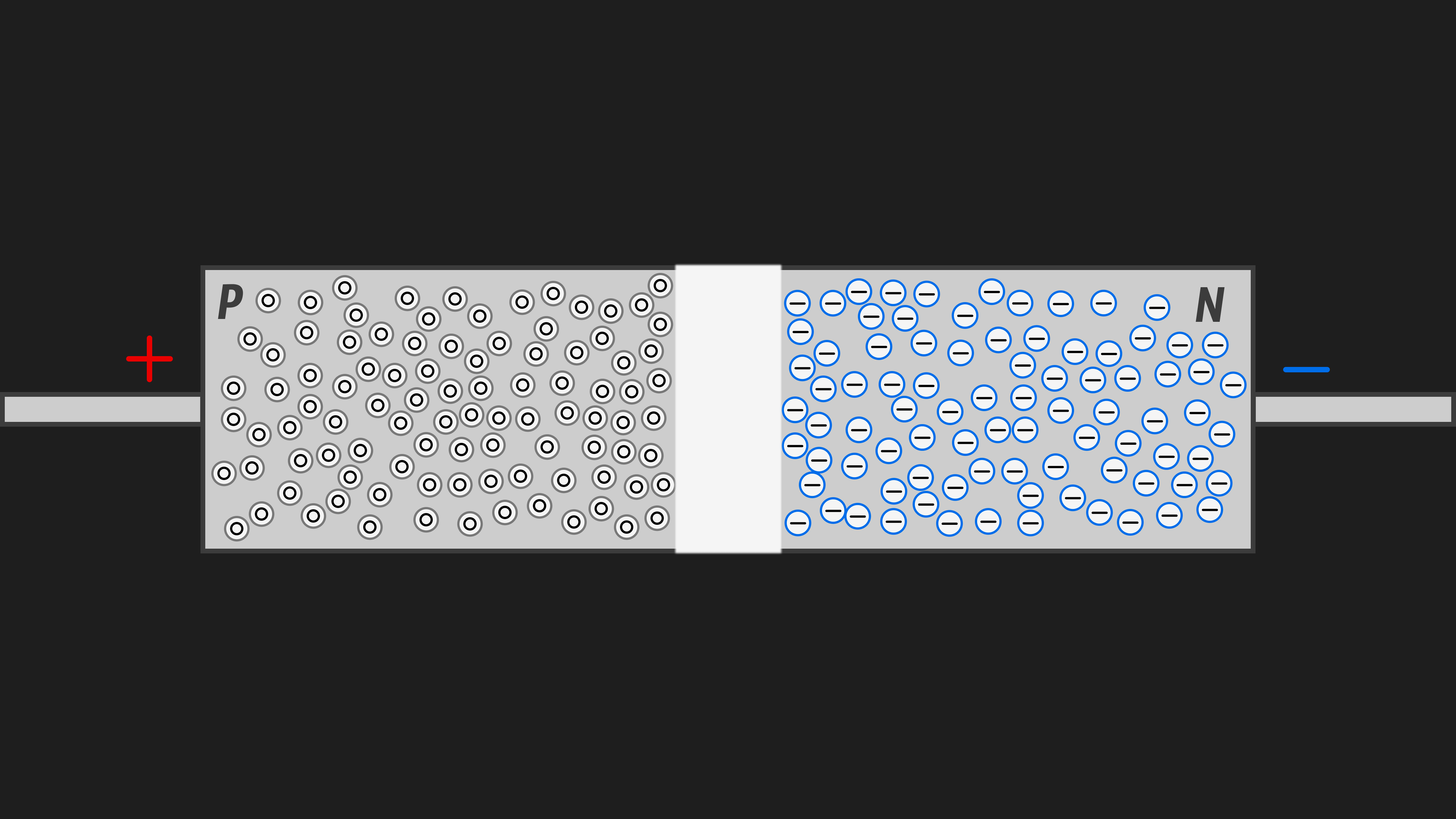
Now let's try applying voltage to our "sandwich" — positive on the left and negative on the right. Obviously, the negative on the right will push electrons from the N region into the P region (since negatively charged electrons repel from the negative terminal), and holes from the P region into the N region, thereby shrinking the barrier region and allowing our sandwich to conduct current (the greater the voltage we apply, the more the barrier region collapses and the better the sandwich conducts current — i.e., the lower its resistance becomes):
Connecting the contacts the other way around, we get the diametrically opposite picture (the reasoning is analogous, just in the reverse direction):
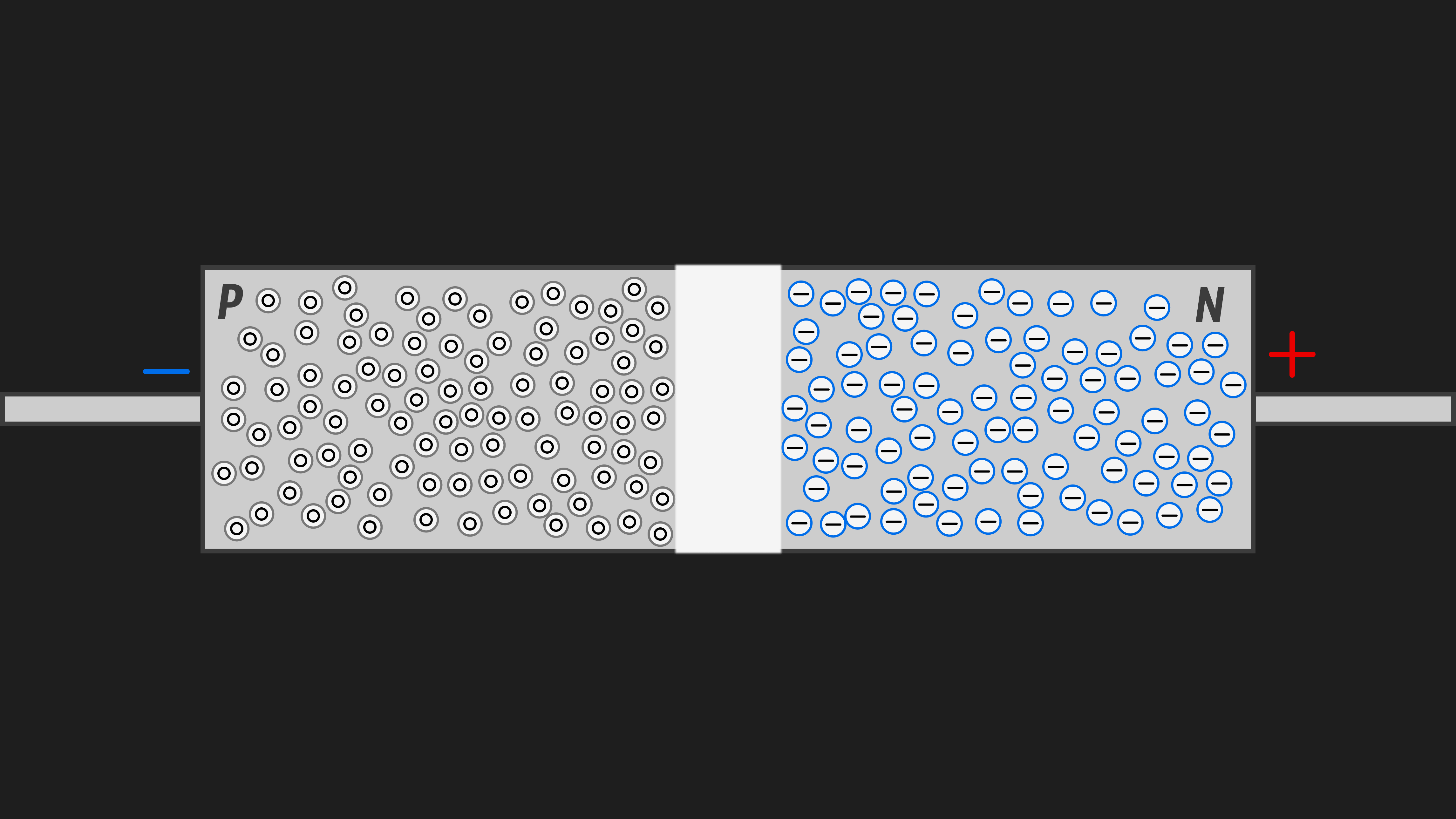
The barrier region expands → resistance increases → the sandwich will conduct current worse the more voltage we apply with this connection, as shown in the animation above.
In the end, we get a device that can pass current in only one direction — such a device is called a semiconductor diode.
Now let's look at a semiconductor triode (a triple sandwich):
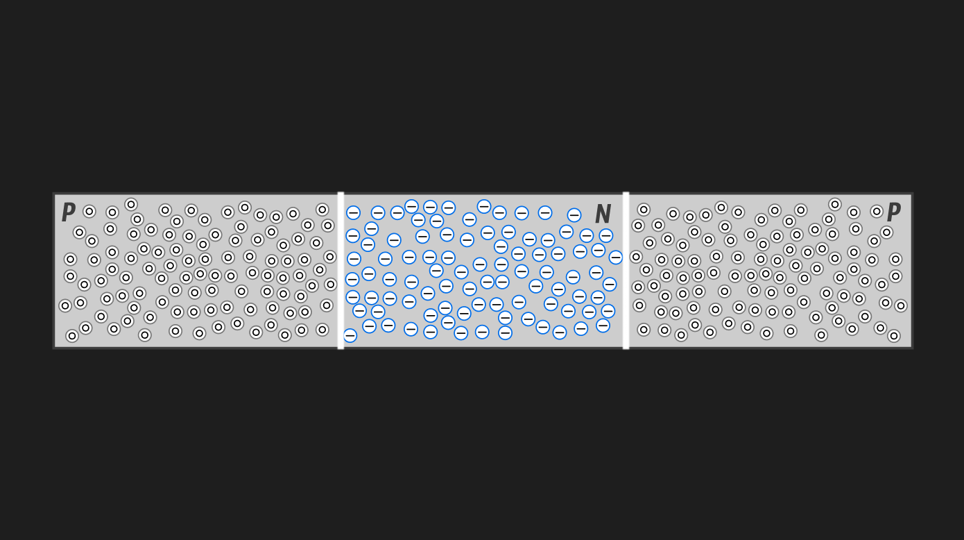
I think even without animation it's clear that no matter how we connect it, it won't conduct current in any case.
We get a p-n-p junction. Connecting, say, negative on the left and positive on the right, only the left barrier region will narrow; the right one will expand, blocking charge carriers. Connecting the triode the other way around, only the left one will expand and now it will be the reason current won't flow through this element.
You can easily understand this by comparing our triode with the two animations above and figuring out which regions will narrow and which will expand with each connection.
It might seem that the triode is useless since under no circumstances will it conduct current (essentially acting as an insulator, just an unnecessarily complex one), but in reality there are ways to make it conduct current (more precisely, this ability can be controlled). Such a controllable triode is called a transistor!
I strongly recommend watching this video, which I largely used as the basis for writing this section. It's also in the references.
What Is a Transistor?
A transistor is an electronic component used to control current in electrical circuits.
It's simply a switch — but not a mechanical one; it's electronic, controlled by external voltage. Such a switch contains no moving parts, is very fast, and can be made very, very small. All these advantages have proven themselves excellently in microelectronics and computer technology.
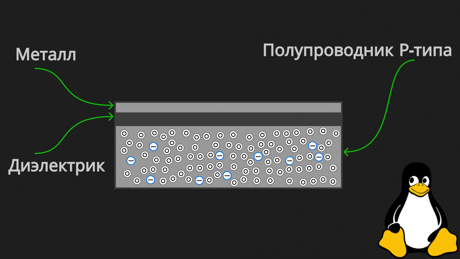
We will examine the field-effect transistor (FET), which is precisely what is used in RAM cells. It's called a field-effect transistor because it is controlled by the field created by voltage applied to the transistor's gate (we'll look at this very soon).
And here is the field-effect transistor itself:
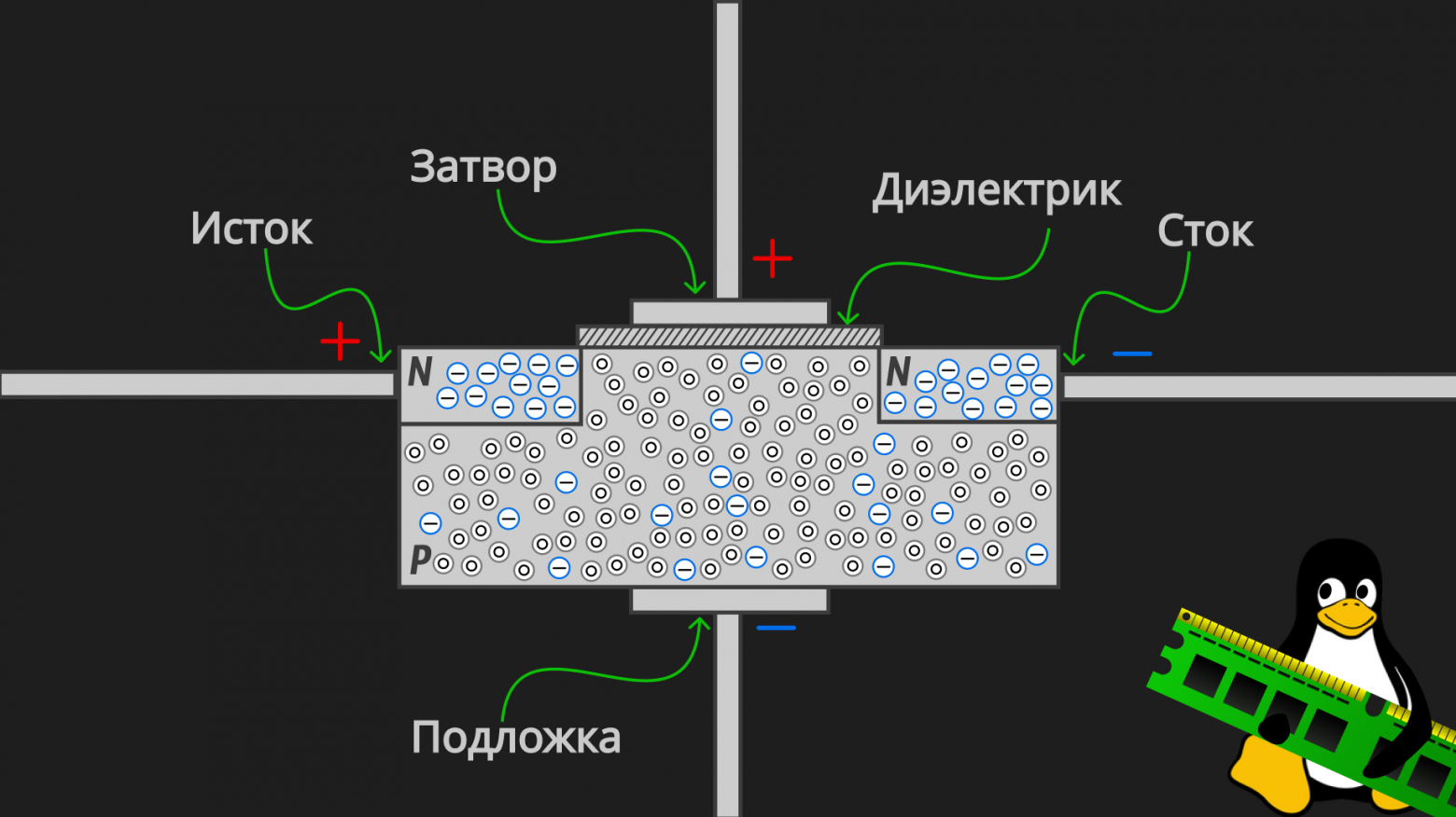
A field-effect transistor consists of two small fragments of semiconductors of one type (N-type in the picture above), embedded into a semiconductor of the other type (P-type in the picture above).
Yes, the P-type semiconductor does have free electrons — obviously — it's just that the number of holes predominates there, as follows from the definition. Earlier we drew semiconductors with only holes or only electrons just for clarity. This is important!
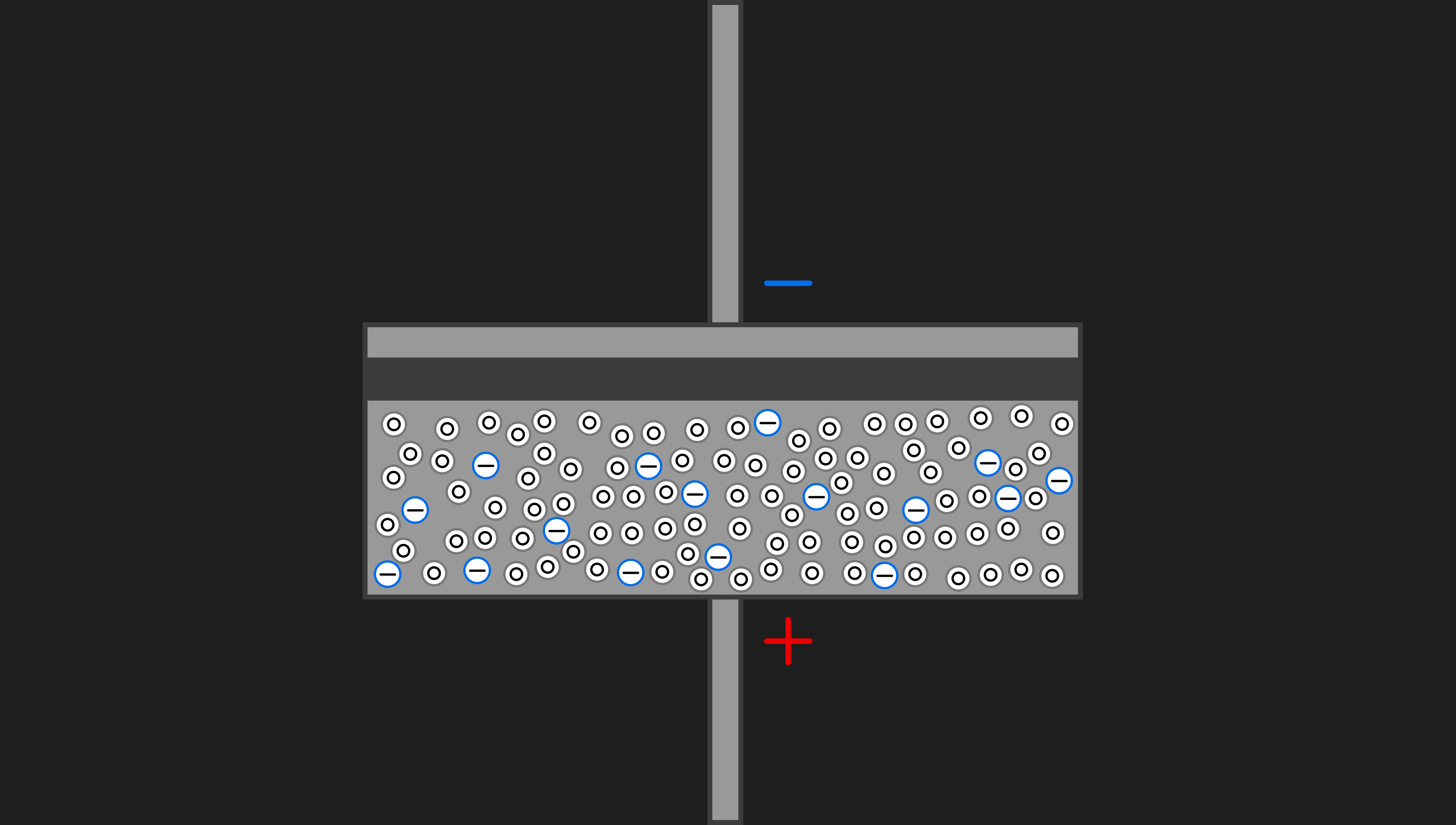
We connect our main circuit (source/drain) through which current flows to the N-type semiconductors (see picture above). However, as we saw earlier with the triode, current will not flow through such a circuit, so we need the gate with the substrate — two contacts at the top and bottom (picture above). Moreover, between the top contact and the semiconductor, there is an insulating (dielectric) plate that doesn't conduct current under any conditions, because the transistor is controlled precisely by the field! As we already said, that same "thing" that strives to restore the harmony of charges (we'll see this in the animation below).
By applying voltage to the vertical contacts (gate and substrate), an electric field arises, under whose influence the few electrons from the P-type semiconductor begin to be pulled upward, closer to the gate:
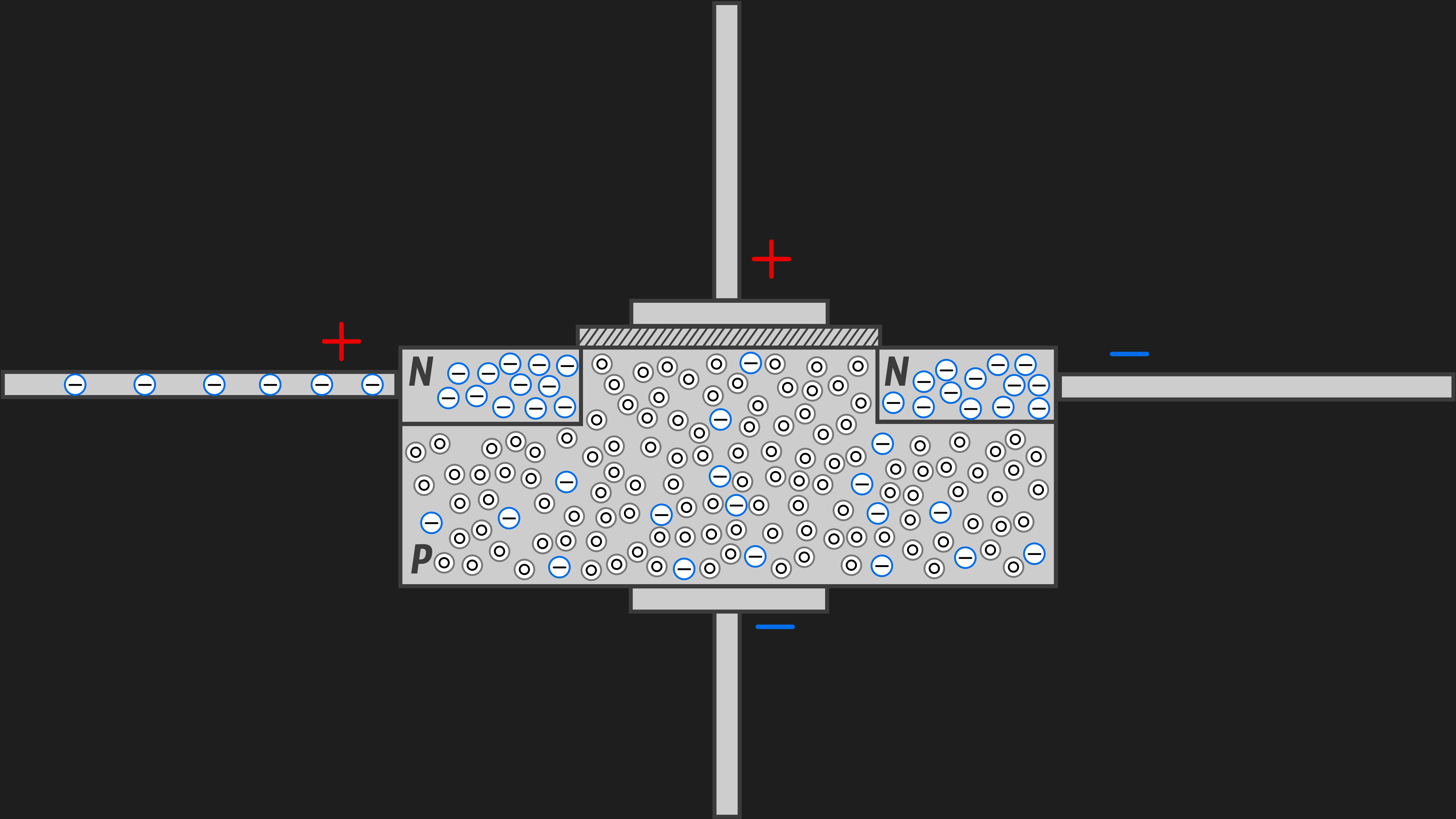
Simply put, electrons will be attracted to the positive charge at the gate (since opposite charges attract), while holes will be repelled (I'll repeat once more — holes don't actually get repelled, they're not real particles. Holes form in the place of electrons that were "attracted" to the gate. But visually, you can say the holes were repelled).
What do we see in the animation above? Although the P-type semiconductor overall has far more holes, in the narrow region near the gate (the top contact) and between the two N-type semiconductors, the concentration of electrons becomes greater than the concentration of holes.
Essentially, in this local region, the P-type semiconductor becomes an N-type semiconductor (or more precisely, a conducting N-type channel forms). Because of this, a conductivity "bridge" forms, since N-type semiconductor conducts current excellently (this is shown clearly in the animation above).
Therefore, by applying voltage to the input and output (source/drain) of our transistor (triode), current will flow through it!
Hooray! We've figured it out, essentially creating the definition of a transistor. A transistor is a device where current flow between the ends/contacts (source and drain) depends on whether there is voltage on the third contact (gate). This way, by applying a small voltage to the gate, you can very easily control the current in the circuit.
Why? For example, to create basic logic gate elements: AND, OR, NOT. And through them, by Post's criterion, you can express any Boolean function and, consequently, build a computer :) But that's a topic for another article...
But a RAM cell doesn't consist only of a transistor — it consists of a transistor and a capacitor. Let's quickly figure out the capacitor and finally move on to the most interesting part about the structure of a RAM stick!
What Is a Capacitor?
A capacitor is an electronic component capable of accumulating electric charge and storing it for some time. That's it :)
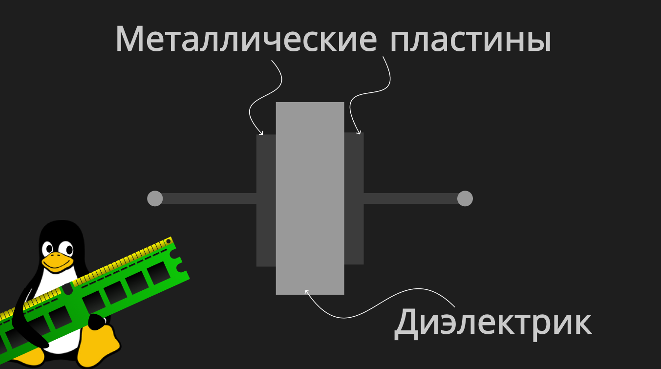
A capacitor consists of two metal plates placed close to each other, with an insulator (dielectric) between them.
Let's break down its charging process step by step:
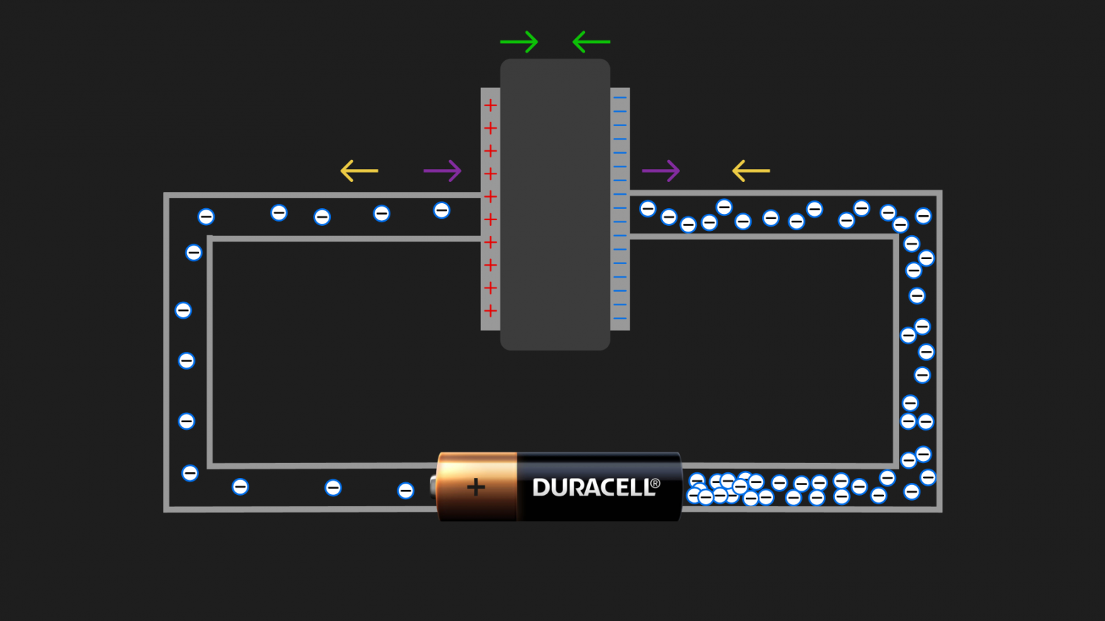
The battery, as we've already understood from the simple circuit with a lamp above, "sucks" electrons from one part of the circuit (creating a deficit of electrons there) and "spits" them into another (creating an excess). Since the plates are made of metal (which is a conductor), the right plate charges negatively (excess of electrons) and the left one charges positively (deficit of electrons — meaning the total charge of the atomic nuclei of the metal in the left plate exceeds the total charge of electrons in it).
Now look at the arrows in the picture:
- Green arrows — the oppositely charged plates, as they acquire charge, begin to influence each other. The positively charged plate will attract electrons from the negatively charged plate, while the negatively charged plate will create a repelling force acting on the remaining electrons in the positively charged plate — essentially "pushing them out of the plate into the wire" (thereby making the plate even more positive);
- Purple arrows — naturally, sooner or later we will hit the limit of a particular capacitor when it can no longer accept new charge (it simply physically can't hold any more). Then we'll say the capacitor is charged. Charge will stop circulating through the circuit and such a system will reach "equilibrium." The right purple arrow shows that the accumulated negative charge on the right plate repels the electrons that the battery is "spitting out" (since like charges repel), while the left arrow shows that the positive charge on the left plate attracts the electrons that the battery is trying to "suck" from there (since opposite charges attract). This is precisely what causes the current to "settle down" and the system reaches equilibrium;
- Yellow arrows — show in which direction the battery forces electrons to flow.
While the battery (voltage across a section of the circuit) is connected, the charge will be maintained. The amount of charge a capacitor can accumulate is determined by its capacitance, which obviously increases with larger plate area.
As soon as we disconnect the battery, "harmony" will want to restore itself — electrons from the plate with excess will begin flowing toward the plate with deficit, and current will flow through the circuit without any power source. The very fact of the capacitor discharging will create a directed movement of electrons from one plate to the other. And directed movement of charges (in our case electrons) is called electric current!
The capacitors used in RAM differ slightly from regular ones with two metal plates. They are called MOS capacitors (Metal-Oxide-Semiconductor capacitors), which fully reflects their structure:
As we can see, the MOS capacitor consists of three layers:
- Metal (conductor) — the upper layer;
- Dielectric — the middle layer;
- Semiconductor (in the picture above, specifically P-type, but it can be N-type too; the idea is the same) — the lower layer.
Let's apply negative voltage to the upper metal layer. Now it has an excess of electrons, and consequently the negatively charged metal plate will attract holes from the P-type semiconductor (lower layer):
Electrons from the upper layer are attracted to holes in the lower layer, but the dielectric middle layer prevents them from recombining (we've already mentioned this fancy word several times above).
Now the capacitor is charged — we've written a "1"! By applying positive voltage to the plate, the charge will drain from it and the capacitor will discharge — meaning we write a "0," conditionally, since we ourselves choose how to logically interpret the physical properties of the system.
Finally — The RAM Cell Itself
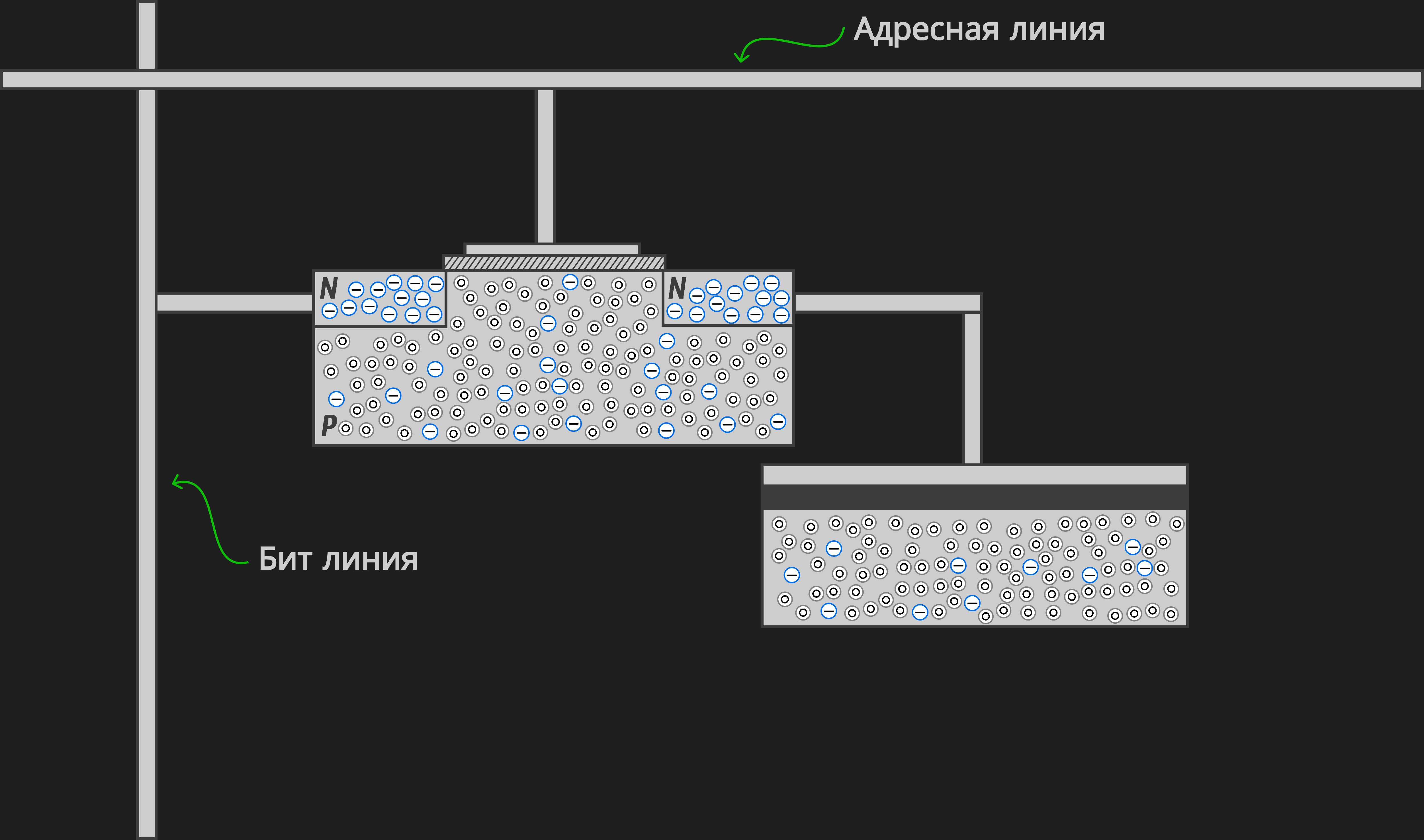
When examining an individual RAM cell — assembled piece by piece from the elements we've already analyzed — we will look at it immediately as part of a larger system, an individual RAM chip. All cells in RAM are linked in a matrix through Bit Line and Word Line contacts.
Very soon we will clearly understand exactly how they are connected, but for now let's close our eyes to this for a couple of minutes and understand the idea as a whole.
A single RAM cell consists of one field-effect transistor and one MOS capacitor, and it is called 1T1C (one-transistor one-capacitor). The transistor's gate connects to the word line, the source connects to the bit line, and the drain connects to the capacitor (specifically, to its upper conducting layer).
And here is the cell itself with its lines (soon we'll understand what these lines are and why they're needed):

IMPORTANT!!! The word line does not touch the bit line; one passes over the other (otherwise such a circuit wouldn't work). Since the picture is two-dimensional, this needs to be clarified.
Let's look at it in action:
When voltage is applied to the word line, the transistor opens (an N-type conducting channel forms) and electrons from the bit line reach the upper layer of the capacitor (the charge passes through the transistor's conducting "bridge"), attracting holes to the upper boundary of the P-semiconductor (lower layer). Now the upper layer of the capacitor has an excess of electrons — it can be viewed as a stored logical "1."
After this, the voltage is removed from the word line, the transistor closes (returns to its baseline state), and the charge that accumulated on the upper metal layer of the capacitor remains trapped there! Since the conducting N-type "bridge" disappears — the electrons are no longer attracted to the gate.
If positive voltage is applied to the bit line, electrons will drain from the capacitor and it will discharge, which can be viewed as writing a "0."
I should note that the MOS capacitor we're examining here is not used in modern RAM chips, but what matters right now is understanding the model itself, the idea. Real RAM uses stack/trench capacitors, which goes beyond the scope of a popular science explanation.
We've come a long way and have earned the right to do this:
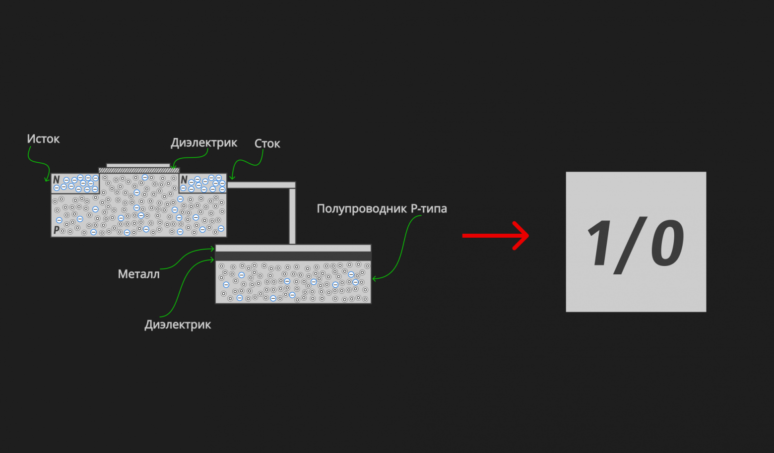
What do I mean? We encapsulate all of our understanding into a square that shows "1" or "0" (charge on the capacitor / no charge on the capacitor). From now on, we will use this to denote a RAM cell. This is necessary in order to look at the structure of RAM from a broader perspective — namely, to understand what memory banks are, how many of them are in one chip, and how many chips are on one stick.
Now, with a complete understanding of how an individual memory cell works, let's move on to the most enjoyable part!
How Are Cells Organized on a Single RAM Stick?
The RAM Model
So, let's first look at the model and then dive into implementation details and the processes of reading and writing. As an example, to fit everything in a picture, let's consider a ridiculously small RAM of 1 Kilobyte (even this article in ASCII encoding weighs almost 100 Kilobytes). By examining a simple model, we will understand how real 16 Gigabyte RAM can be organized.
On one stick we will have 4 chips, and in each chip there are 8 banks:
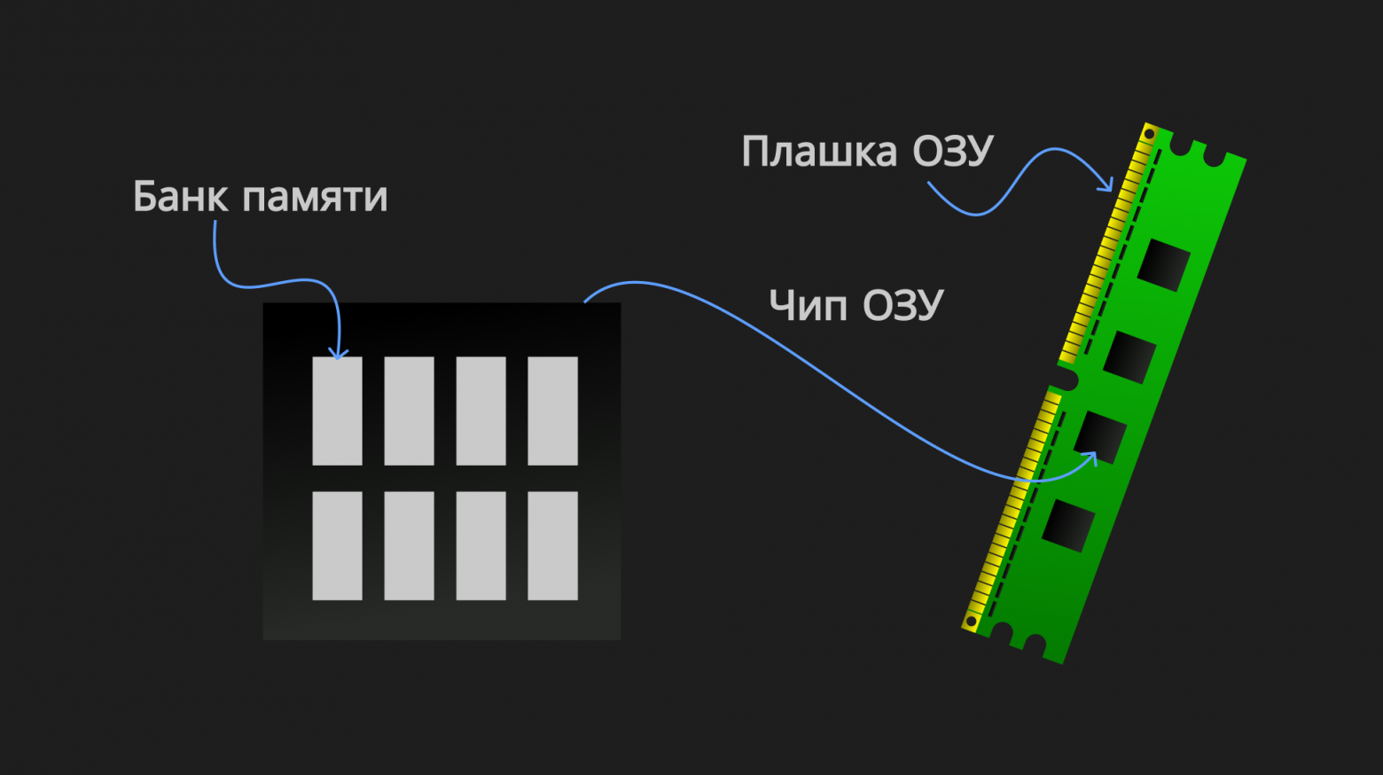
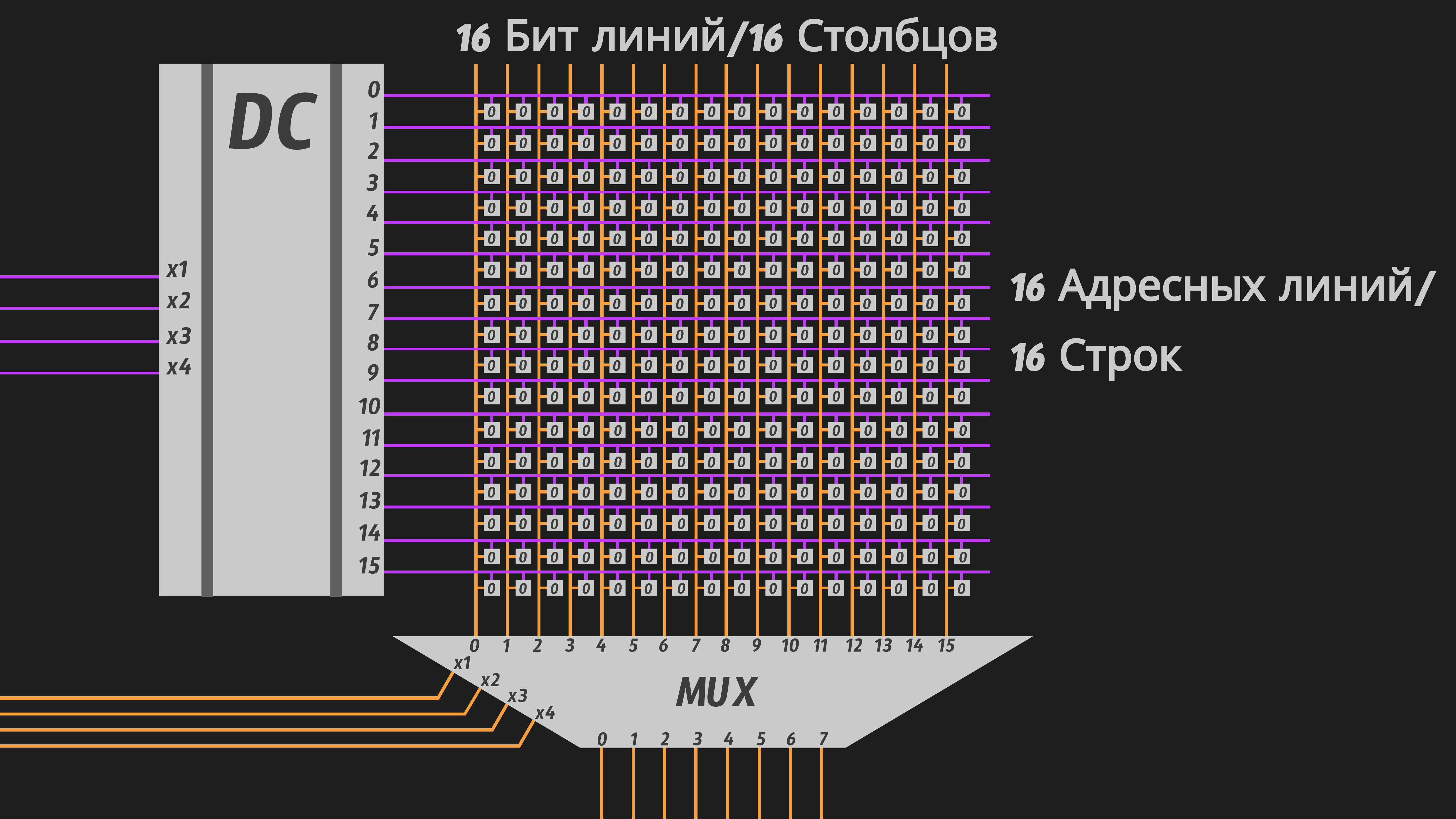
Now let's "drill down" one level — into a memory bank. The cells are organized into matrices called memory banks. Each of our banks (matrices) will have 16 columns and 16 rows:
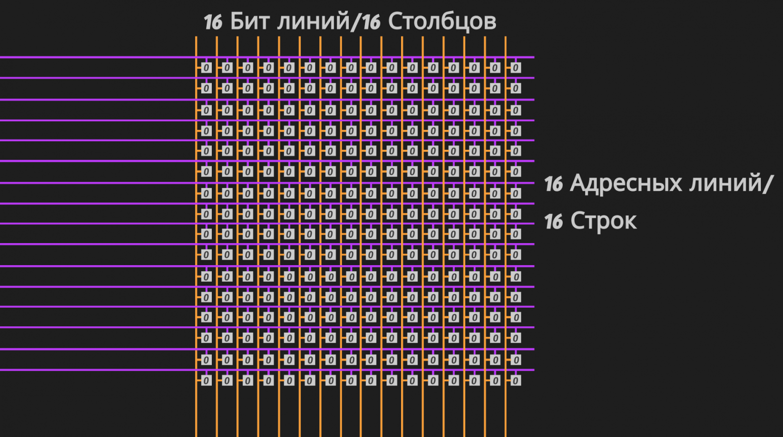
Word lines are shown in purple, and bit lines in mustard yellow. We agreed to denote a single cell (transistor and capacitor) as a square with a "0" or "1." In the picture above, all cells contain "0" — meaning the capacitors in each of the 256 (16 × 16) cells are discharged.
Where does the 1 Kilobyte come from?
- 1 cell stores 1 bit, so our 16 × 16 bank can store 256 bits;
- Each chip has 8 banks, so one chip can store 256 × 8 = 2,048 bits;
- The stick has 4 chips, so the stick overall can store 2,048 × 4 = 8,192 bits;
- 8,192 bits = 8,192 / 8 = 1,024 bytes (since one byte contains 8 bits). 1,024 bytes = 1,024 / 1,024 = 1 Kilobyte.
That's where the 1 Kilobyte comes from!
A real 16 Gigabyte stick might contain 8 chips of 2 Gigabytes each, with 32 banks per chip of 8,192 columns and 65,536 rows. Such a configuration can be used in real RAM sticks. If you carefully calculate, as we did above, you get exactly 16 Gigabytes.
In general, this is the RAM model. All that remains is to understand in general terms how it works.
A Closer Look at the Banks
Let's apply voltage to the fifth word line from the top (we'll mark the voltage in green):
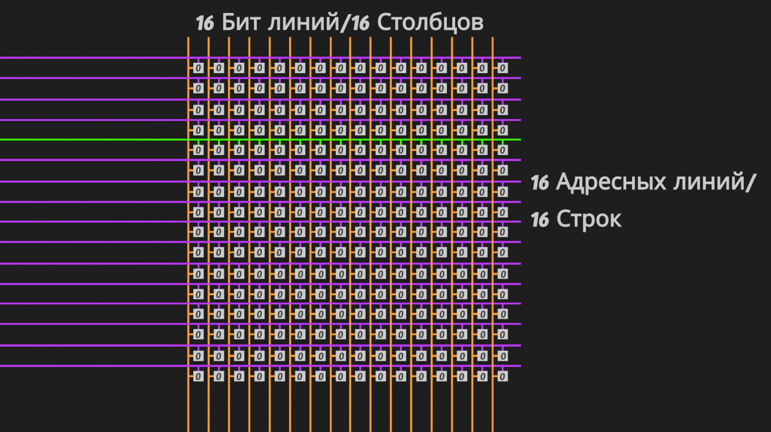
As we examined in detail in the section above, when voltage is applied to a specific word line (in our case the fifth from the top), which is connected to each cell in the row (in our case the fifth row), the voltage on it opens every transistor in the fifth row, providing a "path" to the upper layers of the capacitors in the fifth row's cells.
Now that a specific row is open, the charge from the capacitors will flow through the opened transistors onto the bit lines, and we can read the values of the cells in that particular row. Or we can apply strong/weak voltage to the bit line, thereby writing a value to the cells (we'll see how soon).
But it feels like our model is missing something. We need to figure out how each byte of memory is addressed (since memory is addressed in bytes, not bits — that's 8 bits), what the address itself consists of, and what the bit and word lines connect to.
Decoder and Multiplexer
A decoder and a multiplexer are basic circuit elements. They are very simple to understand and are used in many circuits; RAM is no exception. Let's quickly look at them and finally build the complete picture of a RAM stick. They are built from basic AND, OR, NOT gates, which in turn can be built from transistors (if you don't have an intuitive understanding of what I'm talking about, I strongly recommend watching the second video in the references).
Decoder
It's no secret that to number N objects with numbers in the binary system, we need at minimum  -digit binary numbers. This formula is called the fundamental formula of computer science:

I — the amount of information we can represent in the binary system using N-digit binary numbers (shown visually in the picture below).
Suppose all our 16 rows in a bank need some kind of index so we know "who is who." How many digits do we need for this?
Obviously:

Four digits were just enough:
But what does the decoder have to do with it?
At the logic circuit level, we want a device that takes an N-digit binary number as input (in our case, a four-digit one) and outputs voltage on precisely the line corresponding to the ordinal number of the given binary number (picture above).
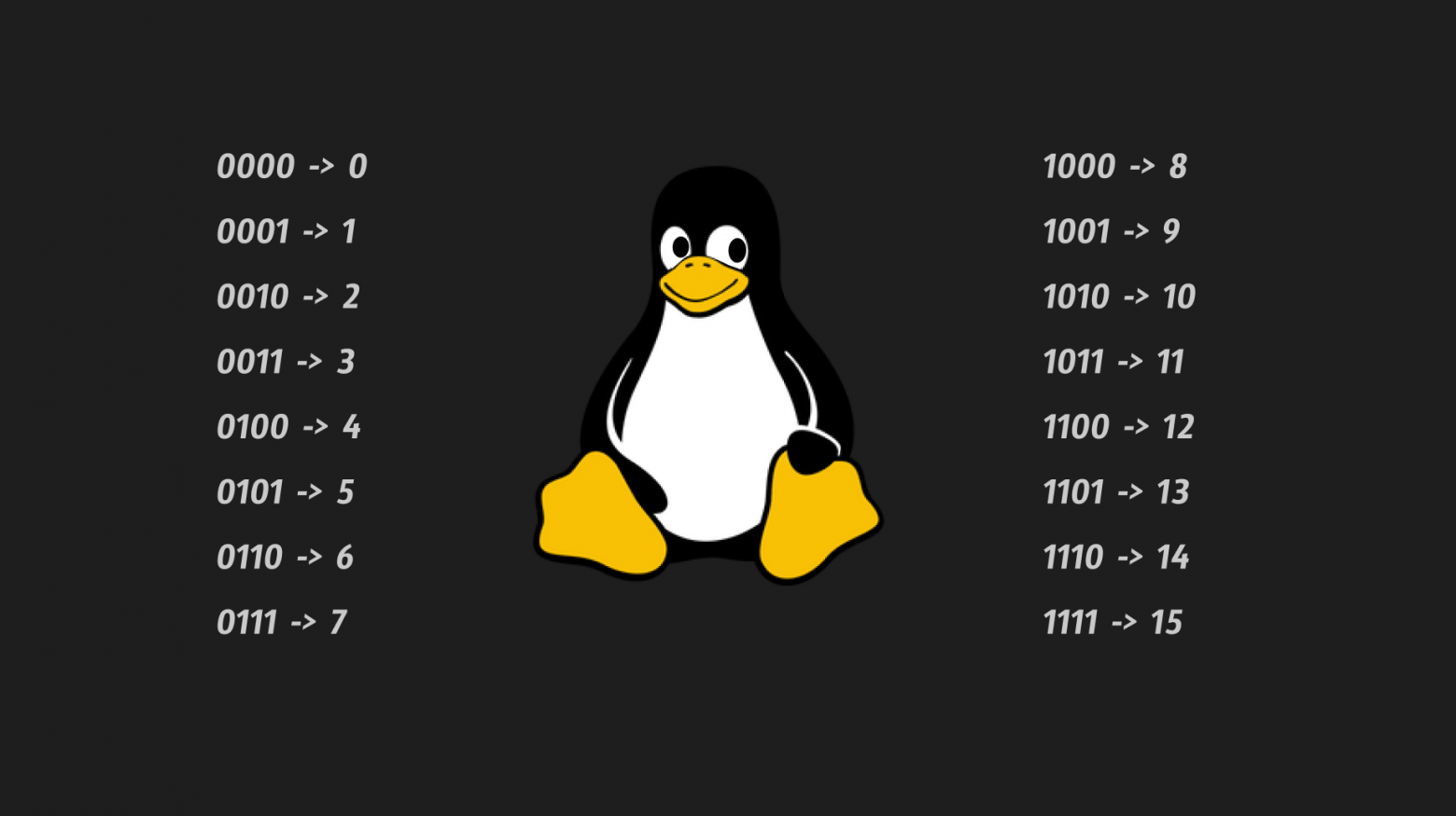
Essentially, a decoder converts a number from binary to decimal:
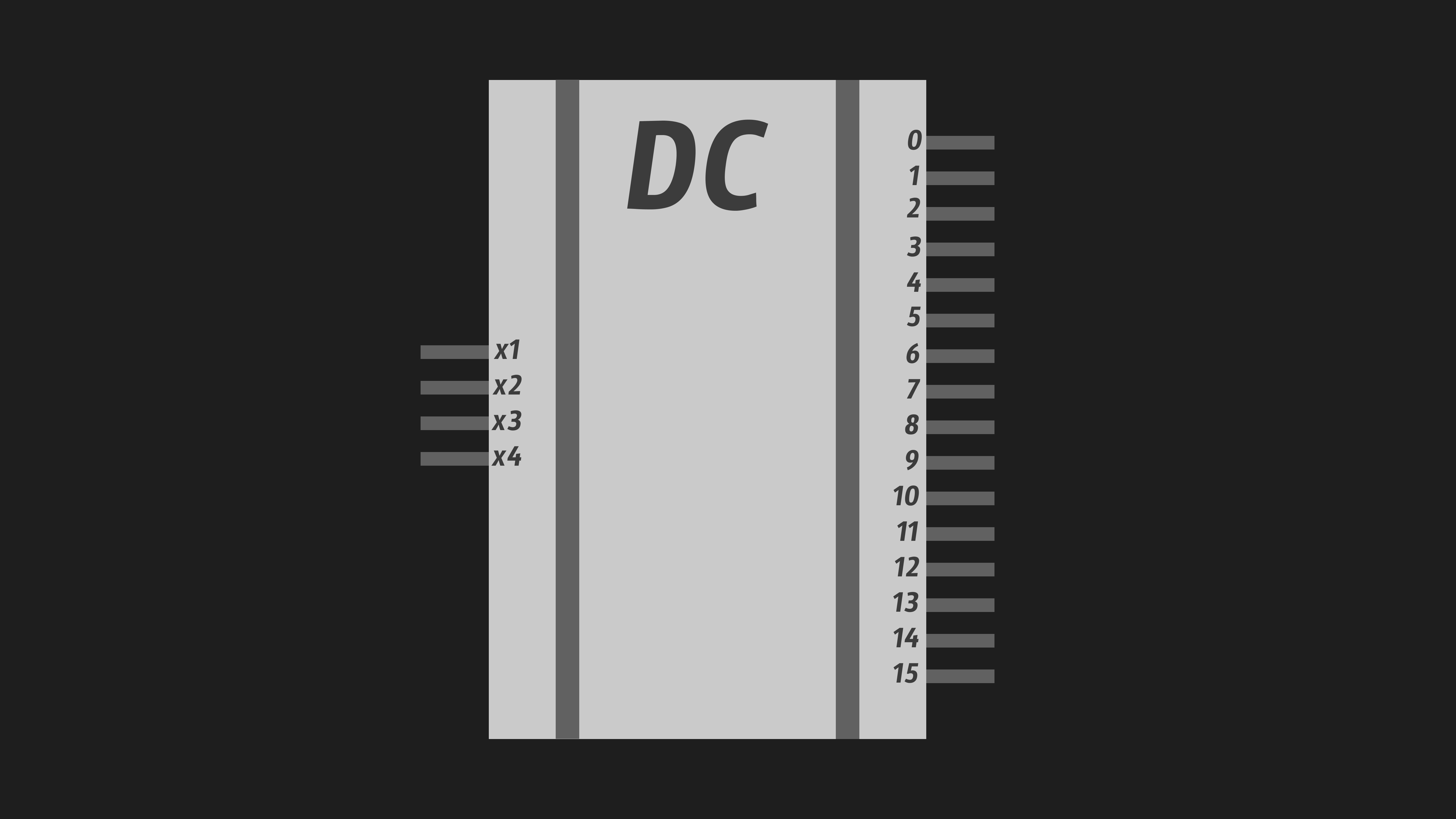
We apply voltage to some of the four inputs (a binary number). Voltage forms only on the output whose ordinal number (starting from zero in decimal) corresponds to the binary number applied to the input (see the penguin picture above).
Perfect! Now we can connect the decoder to the word lines (these will be its outputs) and activate the line we need by specifying its ordinal number at the input!
Multiplexer
Excellent — now we know how to easily activate the word line we need. But when a word line is activated, all cells in the row open (in our simple model drawn above, there are 16 of them in a row; in reality there can be tens of thousands of cells per row). But as I already said, memory is addressed in bytes. We need some way to specify which 8 consecutive cells we need out of these 16 in a row (for example, cells 2 through 9, 7 through 14, or 8 through 15).
The multiplexer helps us here, and it works a bit more interestingly:
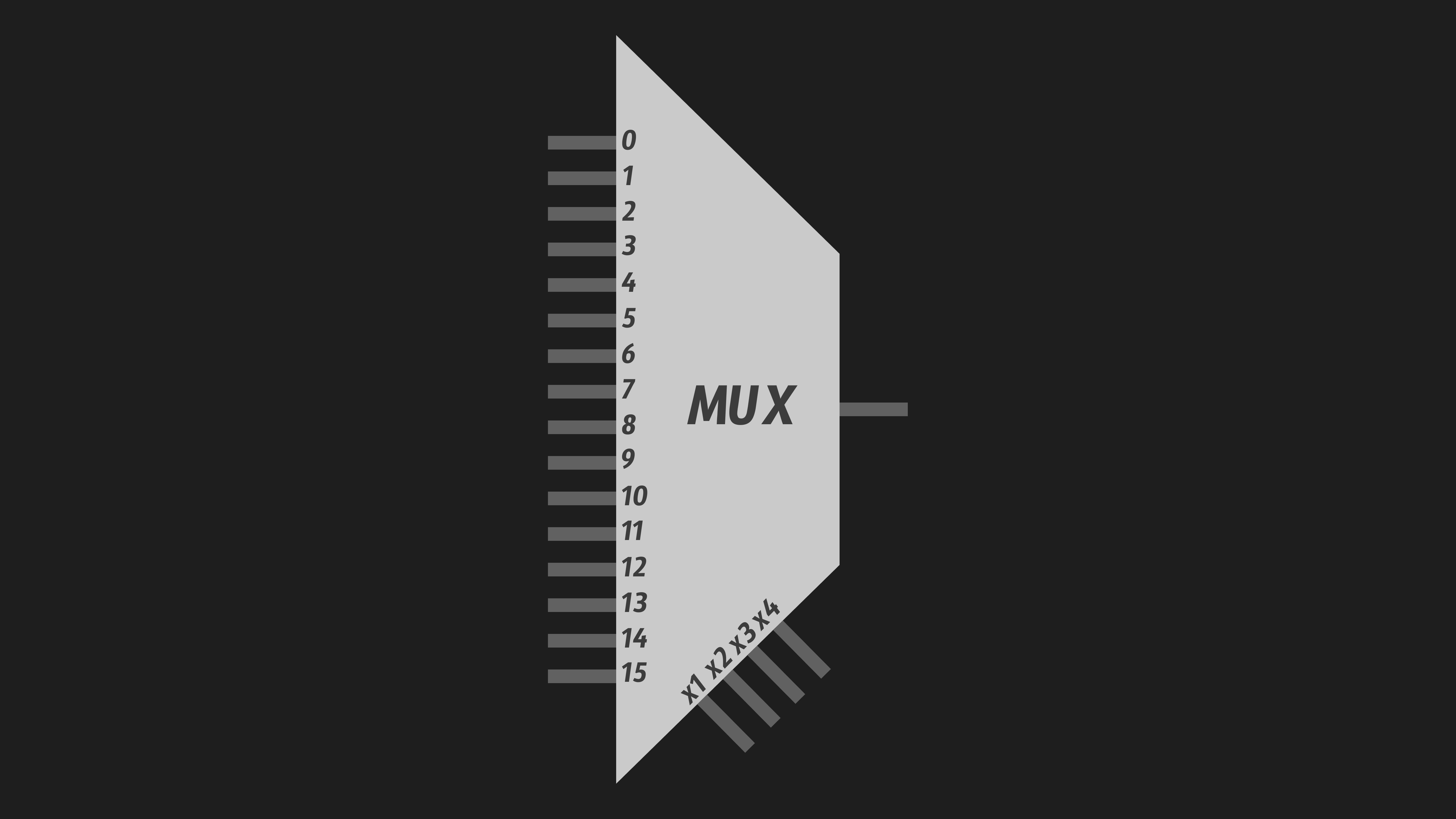
Here we also have inputs on the bottom, called address inputs, and inputs on the left called data inputs (same as with the decoder), but that's not so important. What matters is that all data inputs conditionally have voltage, and depending on the binary number at the address inputs, only the data input whose decimal equivalent matches that binary number (applied to the address inputs) gets "connected" to the output.
Almost the same thing as the decoder, except "under the hood" the multiplexer doesn't just determine the ordinal number (convert from binary to decimal) but also, depending on that number, connects the corresponding input to the output.
This is almost what we need! Above I described a classic multiplexer that from inputs (data inputs), using  address inputs, selects 1 output. But in a RAM bank we need to select a full 8 outputs, since we want to be able to read by bytes. This is achieved simply by combining different numbers of multiplexers of different sizes (in our picture the size is 16:1 — 16 data inputs and one output).
What's important for us is understanding the idea itself. A multiplexer or their "intricate combination" allows selecting M outputs from N inputs, where M < N.
Back to the RAM Chip!
So now the terms row decoder and column multiplexer won't terrify us, and we can add them to the picture we already know. Here's the beauty we get:
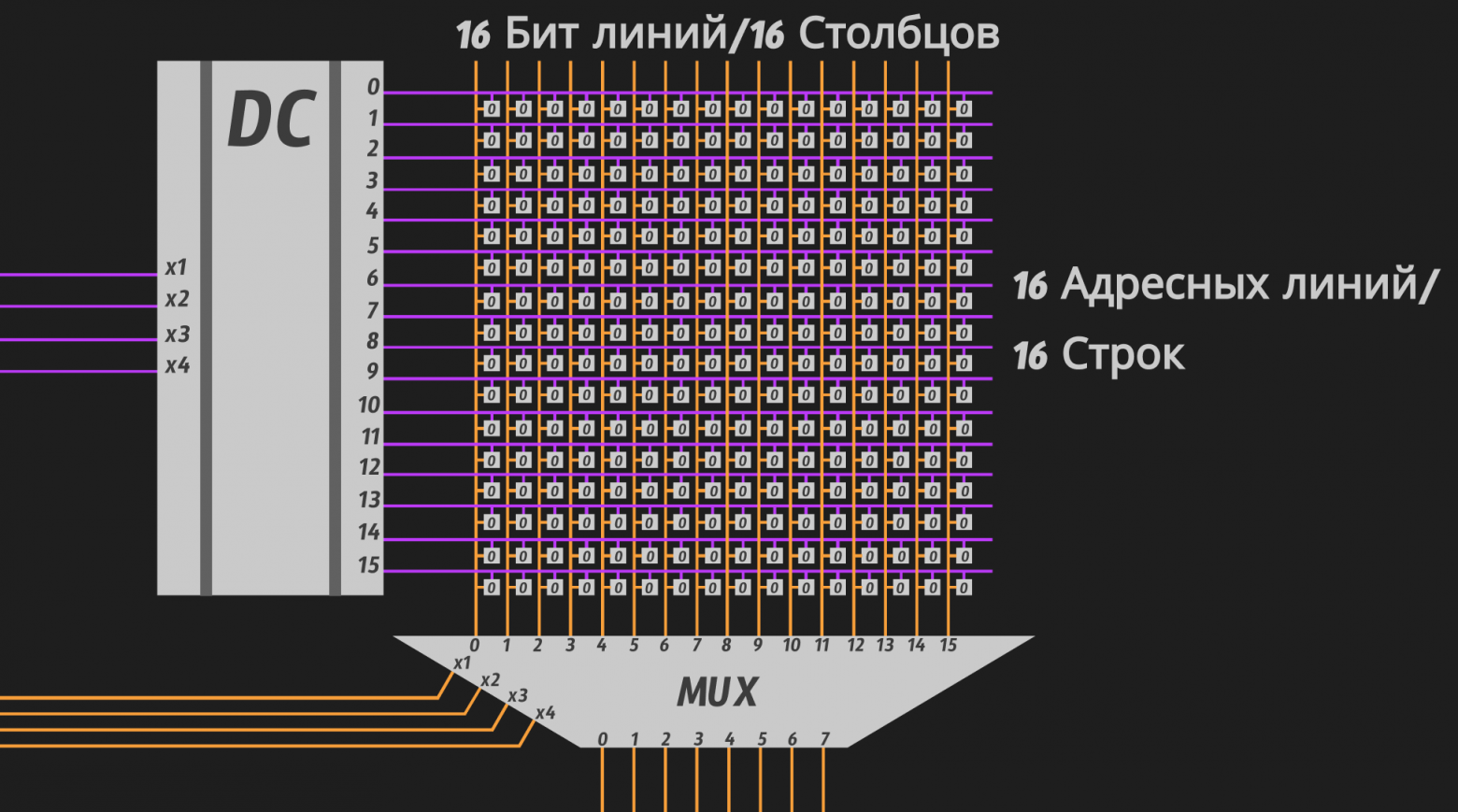
Regarding the multiplexer, let's conditionally assume that the address inputs receive the index of the first data input from which 8 bits will be counted. For example, if we input 0101, i.e., 5 in decimal, the outputs will be bits 5 through 12 inclusive. I think the idea is clear.
Let's Write the Number 255 to Address 01001010111!
We'll look at addressing in the context of a single chip, to avoid overcomplicating an already seemingly confusing picture.
Since we have 8 banks in the chip, 3 bits are enough to number each one:

We have 16 rows and 16 columns, so selecting any one of them requires 4 bits each:

We get an 11-bit address:
[ 3 bits for bank ][ 4 bits for row ][ 4 bits for column ]
Now let's decompose the desired address from the heading, 01001010111, according to our scheme:
[ 010 ][ 0101 ][ 0111 ]
Let's convert each binary number to decimal:
[ bank → 2 ][ row → 5 ][ column → 7 ],
[ 2 ][ 5 ][ 7 ]
So the number 255 will be written to row 5, into the byte starting at column 7 (i.e., into cells/bits 7 through 14) in bank number 2.
When performing a write operation, a write command, an address, and 8 bits (i.e., 1 byte) that we want to write are sent to the RAM chip. Here's what happens in bank number 2:
Here's what happened in the animation frame by frame:
- Voltage was applied to the data inputs of the row decoder (the number 101, which is 5 in decimal) to select the fifth row (activate the fifth word line);
- The required word line was activated, the transistors opened — now if voltage is applied to the bit line, the capacitors will be ready to accept it;
- The number 0111 (7 in decimal) was applied to the address inputs of the column multiplexer. Then the number 255 was applied to the lower contacts (yes, in RAM the multiplexer is bidirectional) (255 in binary is 11111111, meaning all 8 inputs are activated). Our 8 bits are redirected to bit lines 7 through 14 in accordance with the value 0111 that we applied to the multiplexer's address inputs;
- Then the write occurs. At the intersection of the word line and bit lines, the byte we need appears. The capacitors in these 8 cells accumulate charge — they charge up — thereby changing their value to "1";
- Then the voltage is removed from the word line, all transistors in row 5 close, and the charge accumulated on the capacitors remains in a "locked state," as we remember from the previous section.
That's it. Reading happens in an analogous manner, but in reverse. We activate a specific row, the charge from the capacitors of that row's cells flows onto the bit line and reaches the column multiplexer. Then, on the column multiplexer, using the address inputs, we specify which byte in the row we want to pass through the multiplexer and receive it on the multiplexer's outputs (the lower contacts).
It's important to clarify that at any given moment, only one row (one word line) is activated, and the values from its cells flow onto the bit line and reach the column multiplexer's inputs. If we activated two rows simultaneously, it would obviously be a mess, since the values from two capacitors would be mixed on the same bit line, and such an operation would be meaningless. If you didn't understand, I recommend watching the animation above once more carefully or watching this video.
Subtle Points and Important Clarifications We Didn't Cover
Everything mentioned here was omitted to avoid disrupting the narrative flow and inflating the article's volume. It's better to first understand the conceptual model and build context, and then take a couple of steps back and look at the subject with "fresh eyes." That's why I strongly recommend checking out the references at the end of the article!
General Points
Volatility
What we didn't examine is the refresh process — how between different read and write cycles, the smart RAM replenishes its own cells.
Why does it do this? The thing is, we didn't mention a problem related to charge leaking from capacitors. The transistor layer that, in its closed state, "locks" the charge on the capacitor inside the cell — preventing it from leaking to the bit line — is only a few dozen atoms thick. Over time, electrons "seep" through the closed transistor and the cell loses its charge.
Due to the colossally small size of cells achieved through semiconductor technology, compromises had to be made with the constant refresh of cells.
That's why RAM is called volatile — it works if and only if the PC is running, because without constant refresh, the charge from capacitors will leak almost instantly (by human standards) and the RAM will turn into just a piece of silicon.
Reading/Writing
Reading and writing were examined rather conceptually or academically, in general terms. Some details were omitted.
For example, between the column multiplexer and the bottommost row, there should be sense amplifiers, which register the voltage magnitude on the bit line and decide whether it's a "0" or "1." For instance, if the bit line is set to a range from 0 to 1 Volt, corresponding to "ideal" logical "0" and "1," then if the sense amplifier registers, say, 0.74 Volts on a specific bit line, it will treat this as a logical "1" and apply 1 Volt to that bit line to charge the capacitor to the "ideal" value of 1 Volt.
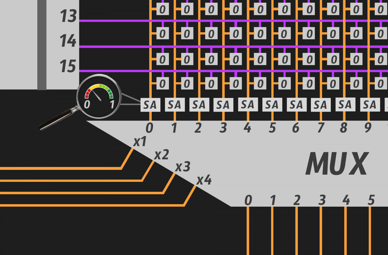
The same applies to a logical "0" — if the voltage on the bit line is less than 0.5 Volts, the amplifier will treat it as "0" and conversely discharge the capacitor.
Also, reading and writing are not as trivial as shown above. Beyond the column multiplexer, there should be read/write drivers/controllers that handle these events slightly differently.
Why Is RAM Specifically "Random Access" Memory?
For a very long time, the English name of RAM confused me. Why is it specifically RAM (Random Access Memory), and what does this "random access" mean?
RAM is called RAM because you can access any cell in approximately the same amount of time, and we don't care where the data is physically located in memory. We know for certain that wherever on the chip the data is stored, we will access it in a roughly fixed amount of time, simply by virtue of RAM's architecture.
I write "roughly fixed" because you could give plenty of examples, delving into specific RAM implementations, showing that access time is not identical. Even if in the case of RAM the access time might differ by negligible fractions of a second, the physical location of the information does not add additional fractions to those already negligible ones — which cannot be said, for example, of an HDD.
Hence "random access" — meaning data can be located in any "arbitrary place" in memory and we absolutely don't care where. RAM (interestingly, in the Russian abbreviation the word "random" is absent) is perceived by us as a black box that can save and return data at specific addresses regardless of their physical location: which chip they're on, which bank within that chip, which row, and which 8 bits of that row constitute the byte we need.
And what about long-term storage?

- In the case of an HDD (a drive with a spinning disk and a read/write head — the first Tux (that's the Linux penguin's name) in the picture above), the physical location of data on the disk matters a lot. Access speed depends on it, since changing the position of the read/write head takes time, even if negligible by human standards;
- In the case of an SSD (the second Tux in the picture above), things are almost like RAM since there are no moving parts as in an HDD, but there are nuances regarding read/write that go beyond the scope of this article and are absolutely unnecessary for understanding memory even at a good level!;
- I'm not even talking about data storage methods like magnetic tape (a long tape with magnetic coating — data is written sequentially; to read the desired block, you need to physically rewind the tape to the right place, meaning there's no fixed-time access at all — the third Tux in the picture above) or magnetic drum (a spinning cylinder where data is written on magnetic tracks, also sequentially).
And even though SSD can also be called Random Access, which makes things even more confusing, these names (like most things in IT) should be treated not as things reflecting the technical side but as things reflecting the historical side. Since the term RAM (Random Access Memory) was coined earlier (1950s) than SSDs (Solid-State Drives), which only became widespread in 2007-2008, back in the distant fifties, RAM was truly the most Random Access of all Random Access :)
In one sentence: Random Access because the access time to any memory cell does not depend on its physical location.
I hope there should be no confusion here now.
Conclusion
Thank you for making it this far! I hope you learned something new and were amazed by the beauty of the inner world of computers — and perhaps you want to study such things further!
What we covered in this article (in bullet points):
- Types of substances: conductors, insulators, and semiconductors from the perspective of the Bohr model of the atom;
- We joined two semiconductors together to get a diode and understood that it can be controlled by external voltage in a circuit;
- Having understood the diode, we also understood the transistor (triode) — the foundation of all modern microelectronics;
- Having analyzed the operating principles of a capacitor, we combined it with a transistor and got a real RAM cell;
- We examined a RAM stick and found that it simply contains several identical chips. We analyzed in detail the structure of memory banks that make up a chip;
- We examined the process of writing and reading in general terms and summarized our findings.
I'd be happy to see comments with additions to the material or pointing out inaccuracies in the article. Thank you once again, and see you next time!
References
YouTube:
- How Computer RAM Works — Branch Education
- The Magic of Transistors: How We Taught Computers to Think Using Pieces of Silicon
- A Special Kind of Matter? What Is the Electromagnetic Field Made Of?
- Semiconductors — Vladimir Kobrin. TsentralNauchFilm [1978]
- Transistors and Their Applications
- How Do Electric Capacitors Actually Work?
Other:
Why This Matters In Practice
Beyond the original publication, RAM: A Comprehensive Guide. Part 1 — The Physical Design of RAM, from Silicon Atoms to Real Chips matters because teams need reusable decision patterns, not one-off anecdotes. A deep-dive into how RAM actually works, starting from the behaviour of individual silicon atoms and ending with the complete architecture o...
Operational Takeaways
- Separate core principles from context-specific details before implementation.
- Define measurable success criteria before adopting the approach.
- Validate assumptions on a small scope, then scale based on evidence.
Quick Applicability Checklist
- Can this be reproduced with your current team and constraints?
- Do you have observable signals to confirm improvement?
- What trade-off (speed, cost, complexity, risk) are you accepting?