What Is a TPU?
A detailed exploration of Google's Tensor Processing Unit architecture, from systolic arrays and XLA compilation to multi-pod scaling with optical circuit switches.
Introduction
Recently, I've spent considerable time working with TPU systems and found it fascinating to observe the stark contrasts in their design philosophy compared to GPUs.
The primary strength of TPUs lies in their scalability. This is achieved through both hardware factors (energy efficiency and modularity) and software components (the XLA compiler).
General Information
In brief, TPU is Google's ASIC that emphasizes two factors: enormous matrix multiplication performance + energy efficiency.
Their history began at Google in 2006, when the company first considered whether to implement GPUs, FPGAs, or specialized ASICs. At that time, only a few application areas required specialized hardware, so the company decided to meet its needs through underutilized CPU resources in its large data centers. However, the situation changed in 2013: Google's voice search function began using neural networks, and calculations showed it would require significantly more compute capacity.
Today, TPUs form the foundation of most of Google's AI services, including training and inference for Gemini and Veo models, as well as deployment of recommendation models (DLRM).
Let's start examining TPU internals from the lowest level.
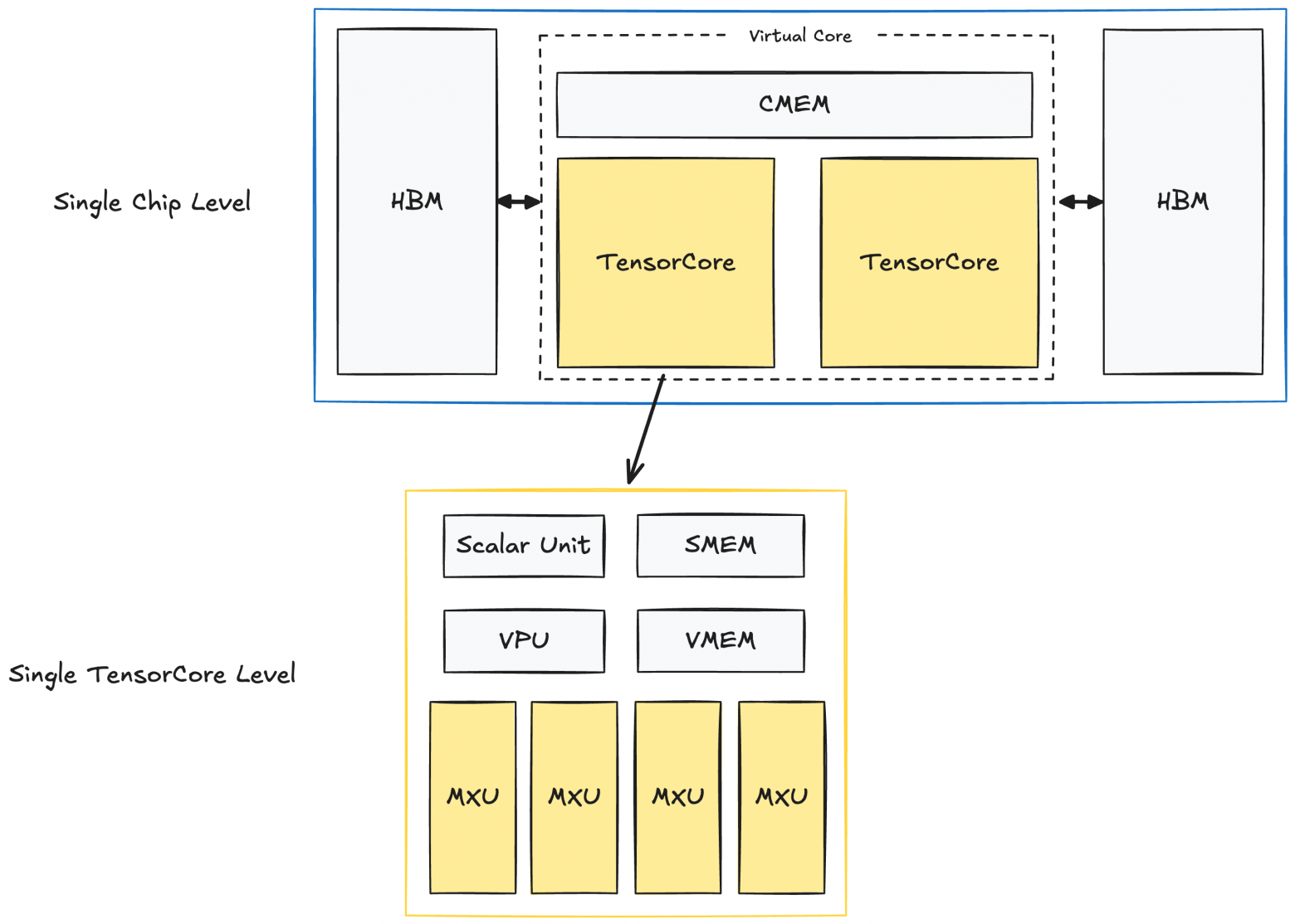
TPU at the Individual Chip Level
In my diagrams, I'll primarily examine TPUv4, though this structure largely applies to newer TPU generations (TPUv6p Trillium; TPUv7 Ironwood specifications hadn't been published at writing).
Here's how a single TPUv4 chip is structured:
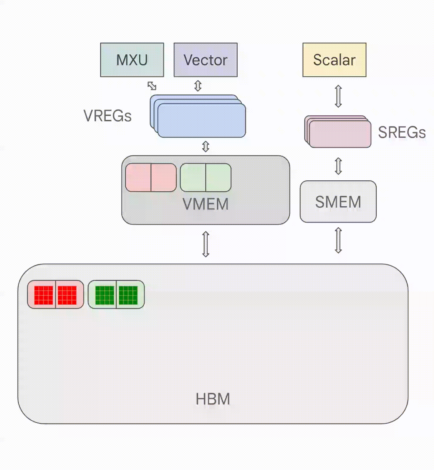
Each chip contains two TPU TensorCore units responsible for compute. (Note: inference-specialized TPUs have only one TensorCore). Both TensorCore units share memory blocks: CMEM (128 MiB) and HBM (32 GiB).
Within each TensorCore are compute blocks and smaller memory buffers:
- Matrix Multiply Unit (MXU): This is the key TensorCore component, consisting of a 128×128 systolic array. We'll discuss systolic arrays in detail below.
- Vector Unit (VPU): Performs general element-wise operations (like ReLU, element-wise addition/multiplication, reductions).
- Vector Memory (VMEM): A 32 MiB buffer. Before TensorCore can execute computations, data must be copied from HBM to VMEM.
- Scalar Unit + Scalar Memory (SMEM): A 10 MiB unit that directs VPU and MXU operations, handles control flow, scalar operations, and memory address generation.
If you have NVIDIA GPU experience, several observations might seem counterintuitive:
- TPU on-chip memory blocks (CMEM, VMEM, SMEM) are substantially larger than GPU L1 and L2 caches.
- TPU HBM is significantly smaller than GPU HBM.
- Apparently far fewer "cores" handle computations.
This contrasts sharply with GPUs, which have small caches (256 KB L1 and 50 MB L2 for H100), larger HBM (80 GB on H100), and tens of thousands of cores.
Before proceeding, recall that TPUs, like GPUs, deliver extraordinarily high performance. TPU v5p achieves 500 teraflops per chip, and with a full pod of 8960 chips, approximately 4.45 exaflops. The new TPUv7 Ironwood reportedly reaches 42.5 exaflops per pod (9216 chips).
To understand how TPUs achieve this, we must examine their design philosophy.
TPU Design Philosophy
TPUs deliver remarkable throughput and energy efficiency through two main pillars and a key assumption: systolic arrays + pipelining, Ahead-of-Time (AoT) compilation, and the assumption that most operations can be expressed in ways that map well to systolic arrays. Fortunately, in the deep learning era, matrix multiplication comprises the overwhelming majority of computations.
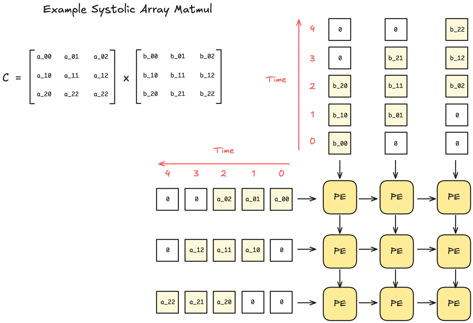
Architectural Solution #1: Systolic Arrays + Pipelining
What is a systolic array?
A systolic array is a hardware architecture consisting of a grid of interconnected processing elements (PE). Each PE performs small computations (like multiplication and summation), then passes results to neighboring PEs.
This architecture's advantage is that after data enters the systolic array, no additional control logic for data processing is needed. Furthermore, in sufficiently large systolic arrays, no memory read/write operations occur except for input/output.
Due to their rigid structure, systolic arrays can only process operations with fixed data flow patterns. Fortunately, matrix multiplication and convolutions fit this mode perfectly.
Additionally, there are obvious opportunities for pipelining computations with data movement. Here's a diagram of pipelined element-wise operations in TPU:
Systolic Arrays' Weakness: Sparsity
As the diagram shows, systolic arrays favor dense matrices (where each PE is active nearly every cycle). However, their limitation is that with equally-sized sparse matrices, there's no performance improvement: the same number of cycles execute, even though PEs operate on zero-valued elements.
Solving systolic arrays' systematic sparsity problem becomes increasingly critical if the deep learning community adopts more uneven sparsity patterns (like MoE).
Architectural Solution #2: Ahead of Time (AoT) Compilation + Reduced Cache Dependence
This section explains how TPUs achieve high energy efficiency by avoiding caches through hardware-software co-design with TPU + XLA compiler.
Traditional caches accommodate unpredictable memory access patterns. Different applications have vastly different memory access patterns. Essentially, caches enable hardware flexibility and adaptation to broad application domains. This flexibility largely explains why GPUs proved so versatile compared to TPUs.
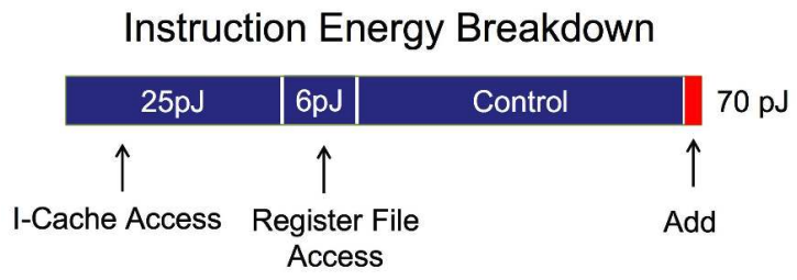
However, cache access (and memory access generally) requires substantial energy. Below is an approximate estimate of chip operation energy costs (45 nm, 0.9 V). This shows memory access and control consume most energy, while arithmetic uses significantly less.
But what if our application domain is specific and its computation/memory access patterns are highly predictable?
Ideally, if a compiler could preknow all required memory operations, hardware would need only buffering without caches.
This is precisely TPU's philosophy, and why TPUs are designed alongside the XLA compiler. The XLA compiler pre-analyzes computation graphs and generates optimized programs.
But doesn't JAX also work well with TPU using @jit?
JAX+XLA on TPU represents hybrid JIT/AOT space, hence the confusion. When first calling a jit-function in JAX, JAX traces it to create a static computation graph. This graph goes to the XLA compiler, where it becomes a fully static binary for TPU. To optimize for TPU, TPU-specific optimizations (like minimizing memory operation count) occur at the final transformation stage.
Be careful though: jit-functions must recompile and cache if executed with different input shapes. That's why JAX underperforms with dynamic padding or for-loops with input-dependent varying lengths.
This approach seems nearly ideal, but practical downsides exist: lack of flexibility and strong compiler dependence.
But why does Google pursue this design philosophy anyway?
TPU Energy Efficiency (TPUv4 example)
The previous energy diagram inaccurately reflects TPU metrics, so here's TPUv4 energy breakdown. Note that TPUv4 uses 7 nm process; 45 nm shown here for comparison.
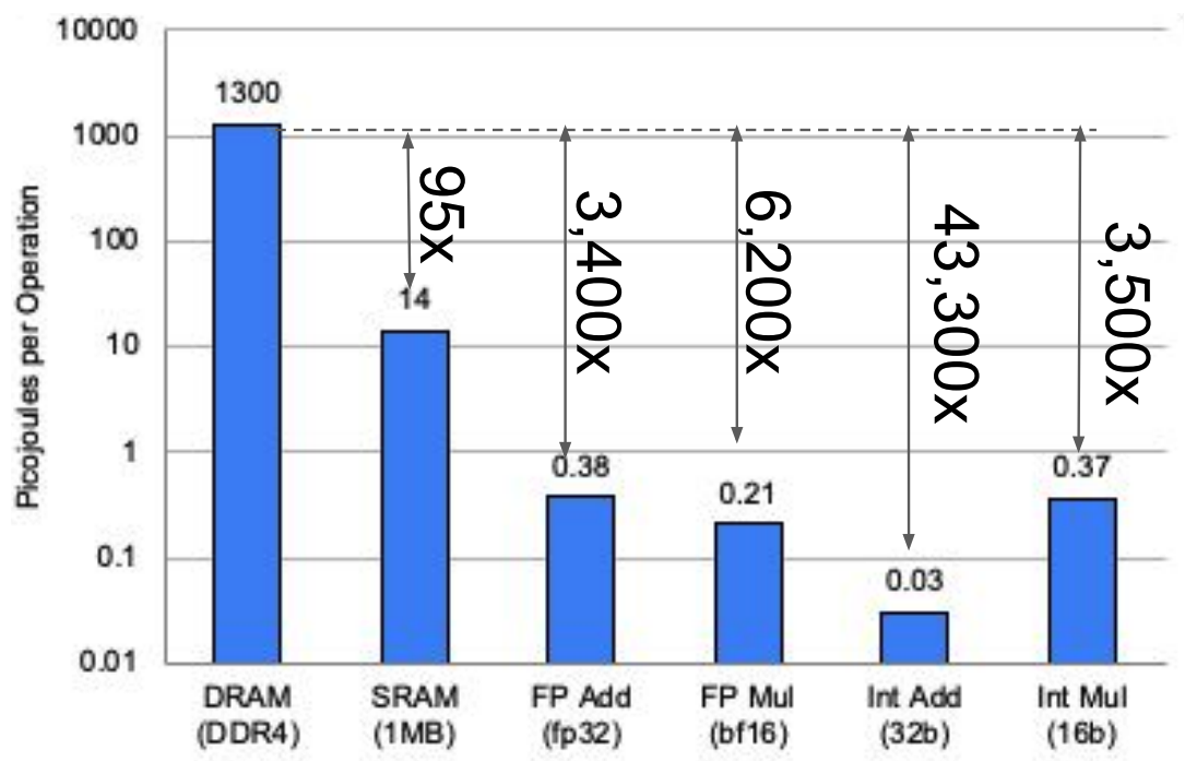
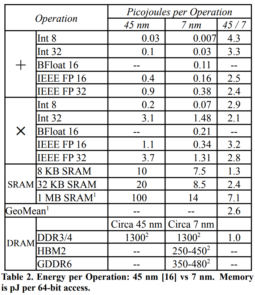
The bar chart shows values, but modern chips use HBM3, consuming far less energy than the DRAM DDR3/4 shown above. Nevertheless, the chart clearly demonstrates memory operations require orders of magnitude more energy.
This connects to modern scaling laws: we eagerly trade increased FLOPS for reduced memory operations. Reducing memory operations compounds optimization benefits, accelerating programs while substantially reducing energy consumption.
TPU at the Chip Set Level
Let's step up and examine how TPU systems function with multiple chips.
Tray Level (or "Board"; 4 chips)
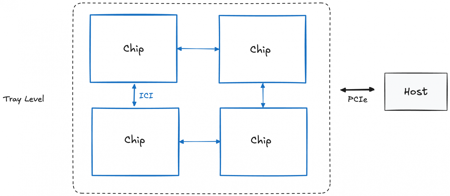
A single TPU tray comprises 4 TPU chips, or 8 TensorCore units (simply called cores). Each tray has its own CPU host (note: for TPU inference, one host accesses two trays since each has only one core per chip).
Host-to-chip communication uses PCIe, but chip-to-chip communication uses Inter-Core Interconnect (ICI) with greater bandwidth.
However, ICI connections extend further, to tray groups. Understanding these requires examining racks.
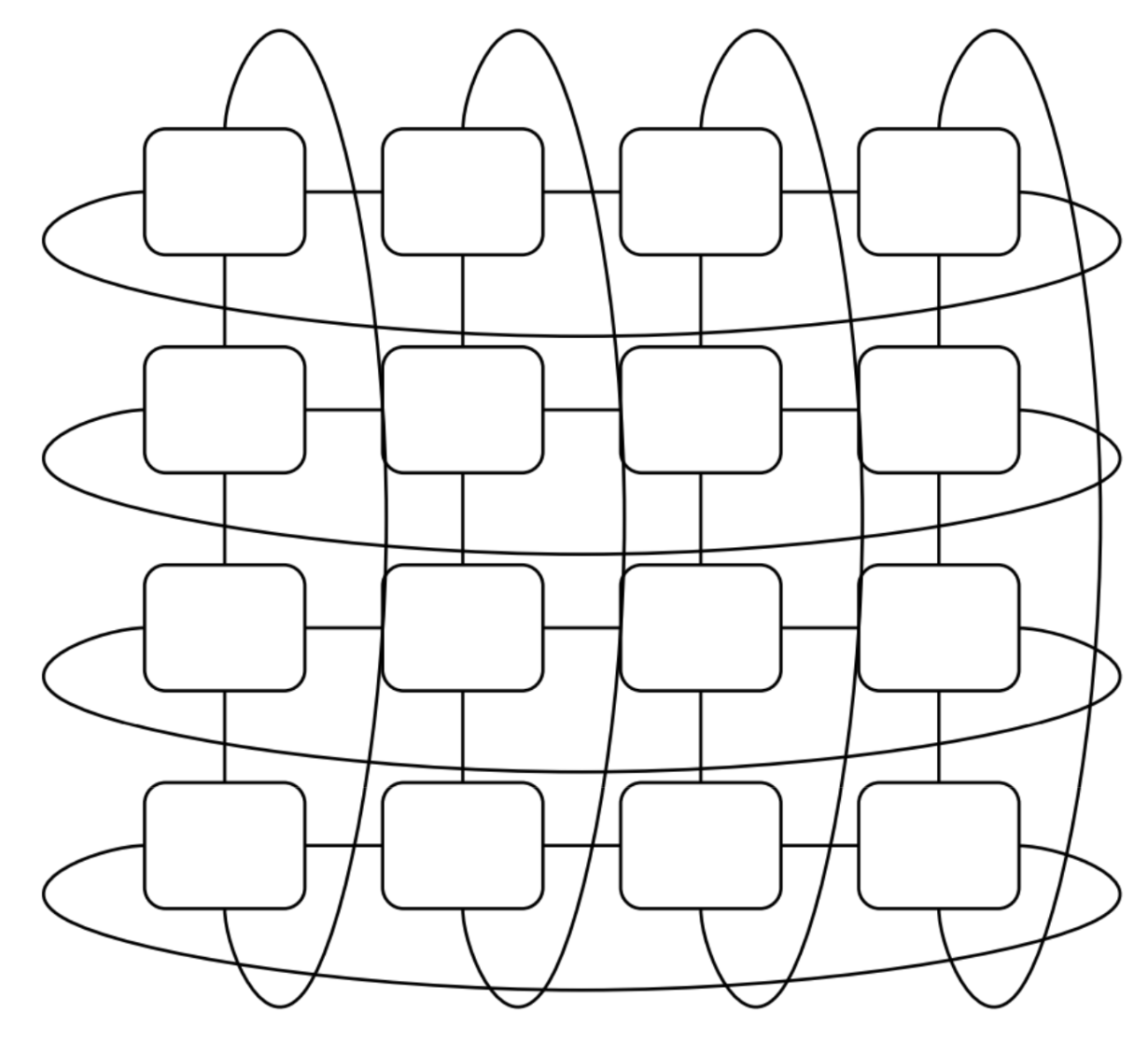
Rack Level (4×4×4 chips)
The most remarkable TPU feature is scalability, observable starting at racks.
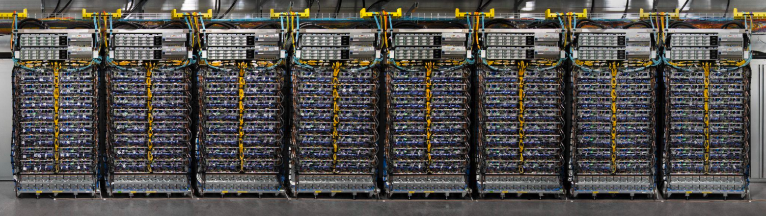
A TPU rack contains 64 TPUs connected in a 3D-torus 4×4×4. Here's an image of 8 TPU racks from Google promotional materials:
Before discussing racks, we must clarify confusing terminology: what's the difference between racks, pods, and slices?
What are the differences between "TPU rack," "TPU pod," and "TPU slice"?
Different Google sources use these terms inconsistently; sometimes "pods" and "slices" mean the same thing. This article uses definitions from Google's TPU research papers and GCP TPU documentation.
- TPU Rack: A physical device containing 64 chips. Also called a "cube."
- TPU Pod: The maximum TPU block connectable via ICI and fiber optics. Often called "Superpod" or "Full pod." For example, a TPUv4 pod contains 4096 chips, or 64 TPU racks.
- TPU Slice: Any TPU configuration from 4 chips up to Superpod size.
The key distinction: racks and pods are physical units, while slices are abstract. Though creating slices requires physical properties awareness, we'll abstract from those for now.
Let's work with physical units: racks and pods. Understanding TPU systems' physical connection methods illuminates their design philosophy.
Returning to TPU racks (TPUv4 example):
One TPU rack contains 64 chips connected via ICI and Optical Circuit Switching (OCS). We essentially combine multiple trays simulating a 64-chip system. We'll return to this topic of combining small parts into supercomputers.
Below is a TPUv4 rack diagram. It's a 3D-torus 4×4×4 where each node is a chip, blue arrows show ICI, and edge lines show OCS:
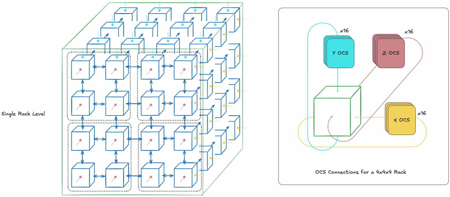
However, examining this diagram raises questions. Why use OCS only on edges? In other words, what's OCS's advantage? Three important advantages exist, with two more discussed later.
OCS Advantage #1: Cyclicity
Increased communication speed between nodes through cyclicity.
OCS cycles TPU configuration. This reduces worst-case hop count between two nodes from N-1 to (N-1)/2 per axis, since each axis becomes a ring (1D-torus).
This effect grows important at scale, since reducing chip-to-chip communication latency is crucial for high parallelization.
Note: Not all TPU have 3D-torus topologies
Older TPU generations (TPUv2, v3) and inference TPUs (TPUv5e, TPUv6e) have 2D-torus topology rather than 3D. However, TPUv7 Ironwood apparently has 3D-torus topology, despite being marketed as an inference chip (this is just my speculation from promotional materials).
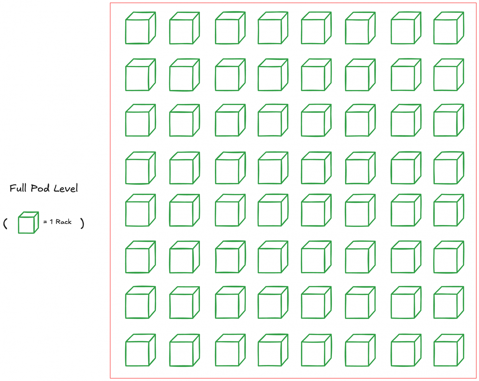
Full Pod Level (Superpod; 4096 chips for TPUv4)
Just as we connected chips for creating TPU racks, we can connect multiple racks creating one large Superpod.
A Superpod is the maximum interconnected (via only ICI and OCS) chip configuration achievable for TPU. Beyond this is the multi-pod level, using slower connections; we'll examine that later.
Maximum size depends on generation; for TPUv4 it's 4096 chips (64 racks of 4×4×4 chips). For newest TPUv7 Ironwood it's 9216 chips.
Below shows a TPUv4 superpod diagram:
Each cube (TPU rack) connects to others via OCS. This enables taking TPU slices within pods.
TPU Slices with OCS
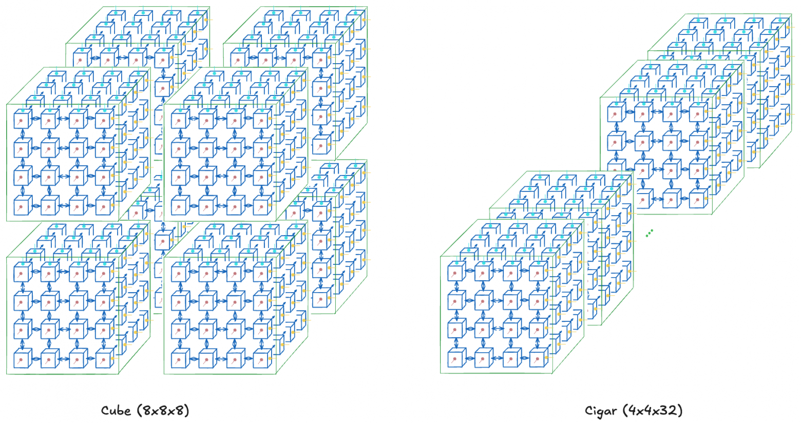
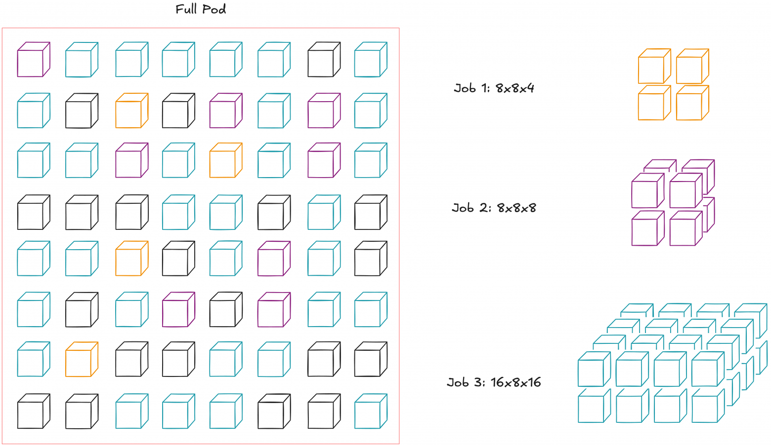
You can purchase TPU subsets within pods, called TPU slices. But even if you need exactly N chips, you must choose from multiple topologies.
Suppose you need 512 total chips. You could buy a cube (8×8×8), cigar (4×4×32), or rectangle (4×8×16). Slice topology choice is itself a hyperparameter.
The chosen topology affects inter-node communication bandwidth width. This directly impacts various parallelization methods' performance.
For example, a cube (say, 8×8×8) suits all-to-all communication used in data or tensor parallelism, having greatest cross-sectional bandwidth. Cigar shape (say, 4×4×32) better suits pipeline parallelism, improving sequential layer communication speed (if one layer fits in a 4×4 chip subslice).
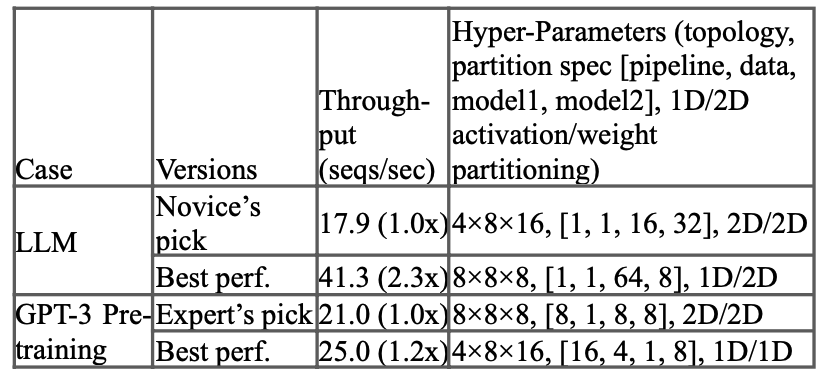
Of course, topology optimality depends on the model; proper selection is separate work. The TPUv4 research paper discusses this, demonstrating how topology increases throughput:
We've examined TPU slices, with another important feature affecting high operational stability.
Due to OCS, these slices needn't be adjacent racks. This is OCS's second advantage (probably most important).
OCS Advantage #2: Non-adjacent (Reconfigurable) Slices from Multiple Nodes
Note this differs from linking multiple nodes simulating non-adjacent slices. Since OCS is a switch, not rigid connection, far fewer physical wires exist between nodes, providing increased scalability (larger TPU pod sizes).
This enables large-scale flexible node configurations. Suppose three tasks run in one pod. This could use naive scheduling, but OCS connections let us abstract node position and treat the entire pod as a "bag of nodes":
This optimizes pod utilization and potentially simplifies maintenance during node failures. Google describes it: "Dead nodes have small blast radius." However, I'm unsure how this affects liquid cooling when only individual nodes disconnect.
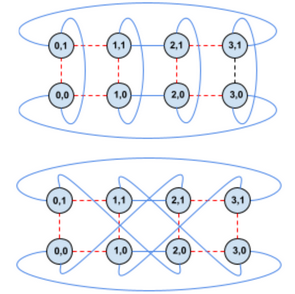
Additionally, this OCS flexibility yields interesting consequences: we can modify slice topology, say from regular torus to twisted.
OCS Advantage #3: Twisted TPU Topologies
Earlier, we saw creating different TPU slice topologies by changing chip dimensions (x,y,z). Now we'll work with fixed dimensions (x,y,z), changing their topologies via connections.
Below shows transitioning from normal cigar-shaped torus to twisted cigar-shaped torus:
With twisted torus, we increase chip communication speed on the twisted 2D-plane. This particularly benefits all-to-all communication acceleration.
Let's examine specific scenarios where this helps.
Training Acceleration via Twisted Torus
Theoretically, torus twisting yields greatest benefit with tensor parallelization (TP), since layers have many all-gather and reduce-scatter operations. Data parallelization (DP) gains less, since training stages have all-reduce operations, appearing less frequently.
Imagine training a standard decoder transformer wanting to leverage substantial parallelism for acceleration. Consider two scenarios.
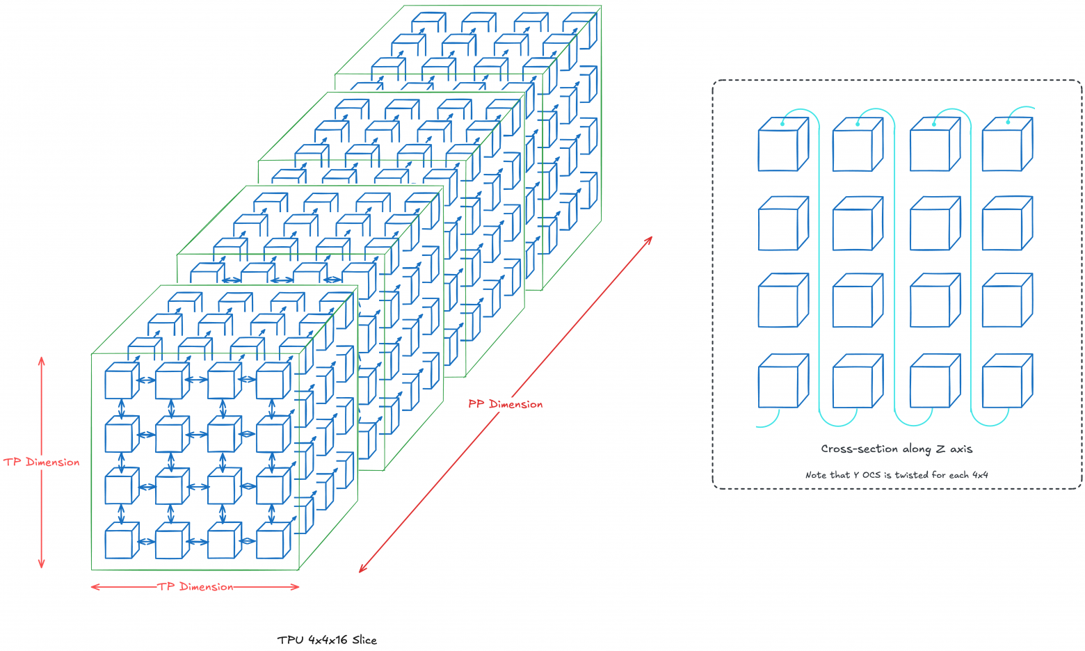
Scenario 1: 4×4×16 Topology (TP + PP; 256 total chips)
Our z-axis will be pipeline parallelization dimension (PP), while 2D TP dimension is 4×4. Essentially, each layer k resides at z=k with each layer divided across 16 chips. If diagrams lack specified connections, standard OCS connections apply (nearest-neighbor connection).
We'll twist the 2D-torus at each z=k, accelerating chip communication within each TP layer. Twisting along PP dimension is optional, since it mainly depends on point-to-point communication.
Note: In reality, torus twisting benefits when chip count exceeds 4×4. We use 4×4 example purely for clarity.
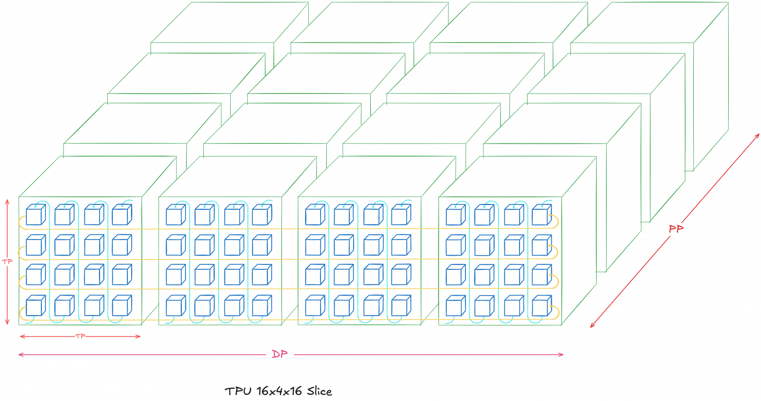
Scenario 2: 16×4×16 Topology (DP + TP + PP; 1024 total chips)
We'll expand the previous scenario, adding a four-chip DP dimension. This means four Scenario 1 instances along the x-axis.
Notice torus twisting limits to each TP dimension in each DP model (the 4×4 2D-plane for each z=k where k=1...16). Looping applies only DP dimension, making each row a horizontal 16-chip ring.
You might notice an alternative 8×8×16 topology exists (DP dimension 2×2), but mixing DP and TP dimensions gets complicated. Specifically, it becomes unclear how organizing OCS looping for the y-axis while fitting twisted toruses for each TP dimension.
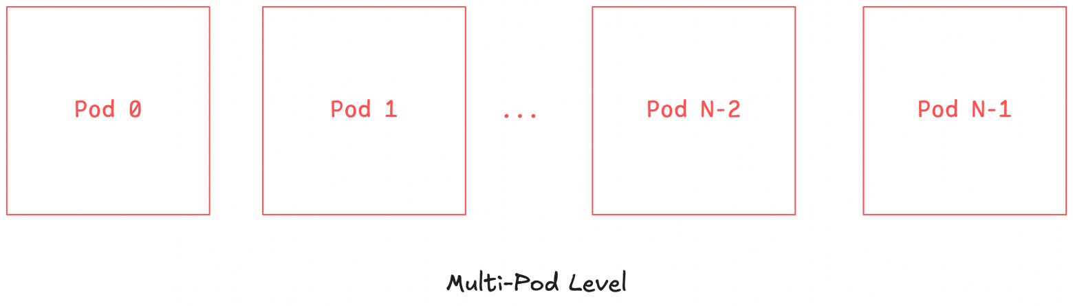
Multi-Pod Level (or "Multi-Slices"; exceeding 4096 chips for TPUv4)
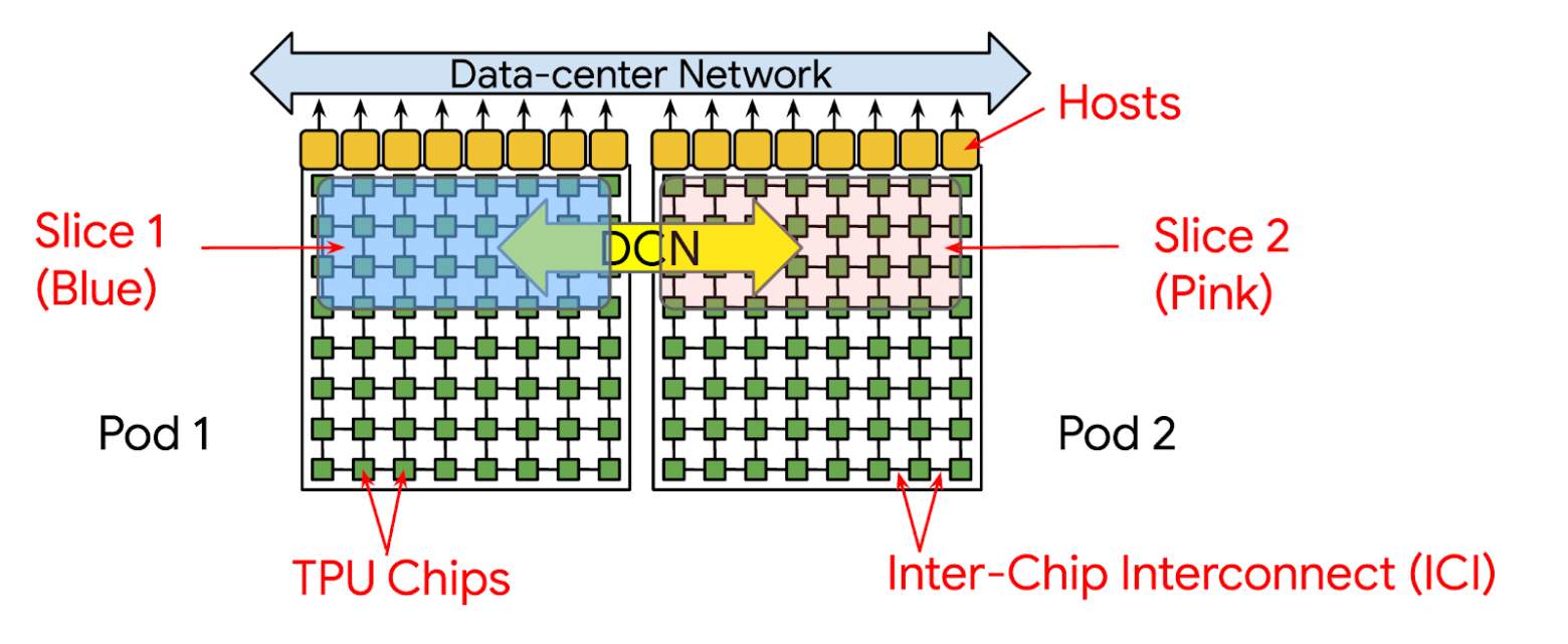
The final TPU hierarchy level is multiple pods (multi-pods). Here, multiple pods function as one large machine. However, inter-pod communication occurs via Data-Center Network (DCN), having less bandwidth than ICI.
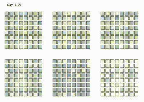
PaLM trained this way. Training 6144 TPUv4s (2 pods) required 56 days. Below shows TPU task distribution across 6 pods: green tasks belong to PaLM, red lack tasks, remainder are other tasks. Each square is a 4×4×4 TPU cube.
Creating such systems presents inherent challenge, yet becomes more impressive remembering developer convenience. Fundamentally, designers prioritized answering: "How maximally abstract hardware/system scaling aspects?"
Google answered: the XLA compiler handles large-scale inter-chip communication coordination. When researchers specify necessary flags (DP, FSDP, TP parallelization dimensions, etc.), XLA inserts appropriate hierarchical communication blocks for existing TPU topology (Xu et al, 2021: GSPMD). The goal is enabling large-scale training with minimal code changes.
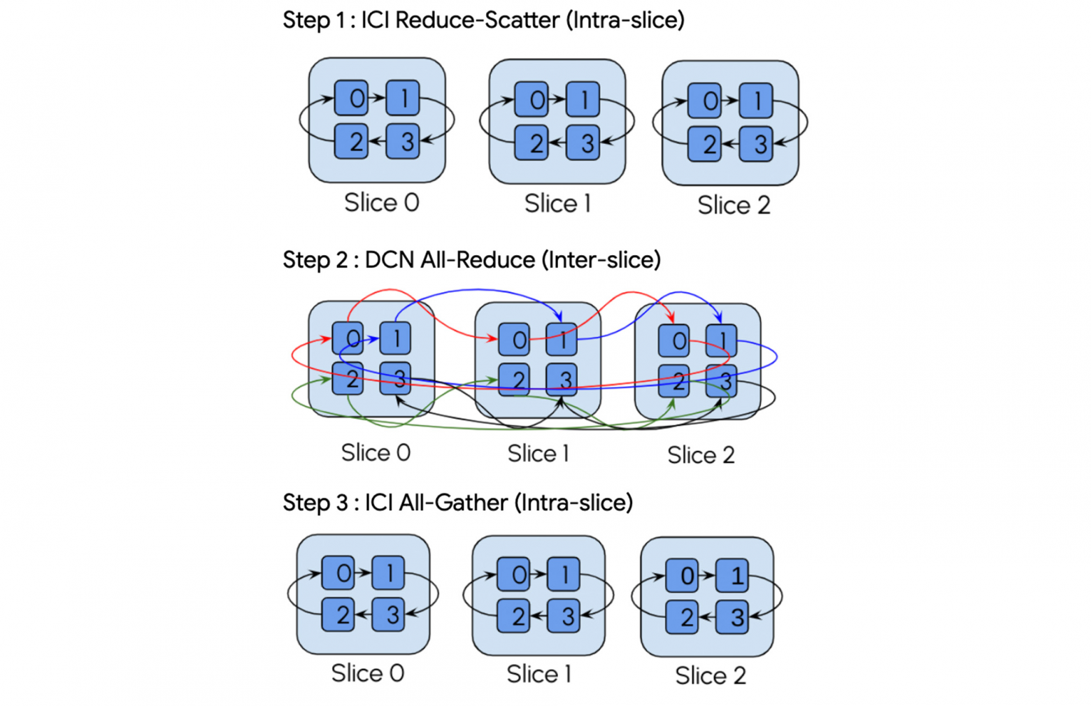
For example, here's multi-slice all-reduce operation breakdown from Google's blog:
It demonstrates XLA compiler handles communication collectives both between and within slices.
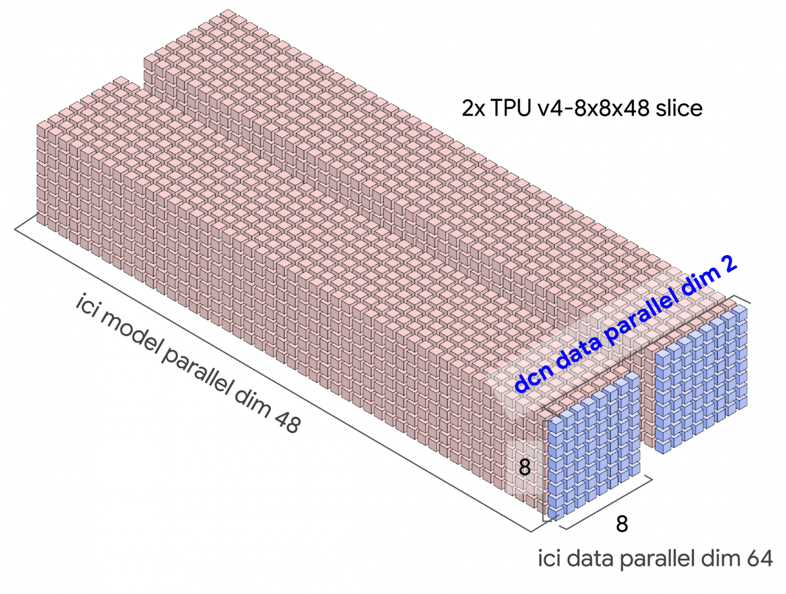
Here's a concrete example: possible TPU topology for model training. Activation communications within slices occur via ICI, while gradient communications between slices occur via DCN (DP dimension DCN):

Relating Diagrams to Reality
I find understanding scale easier observing actual equipment photographs.
If studying Google's TPU promotional materials, you've likely seen this image:
This shows 8 TPU pods where each block is 3D-torus 4×4×4. Each pod row comprises 2 trays, so each row has 8 TPU chips.
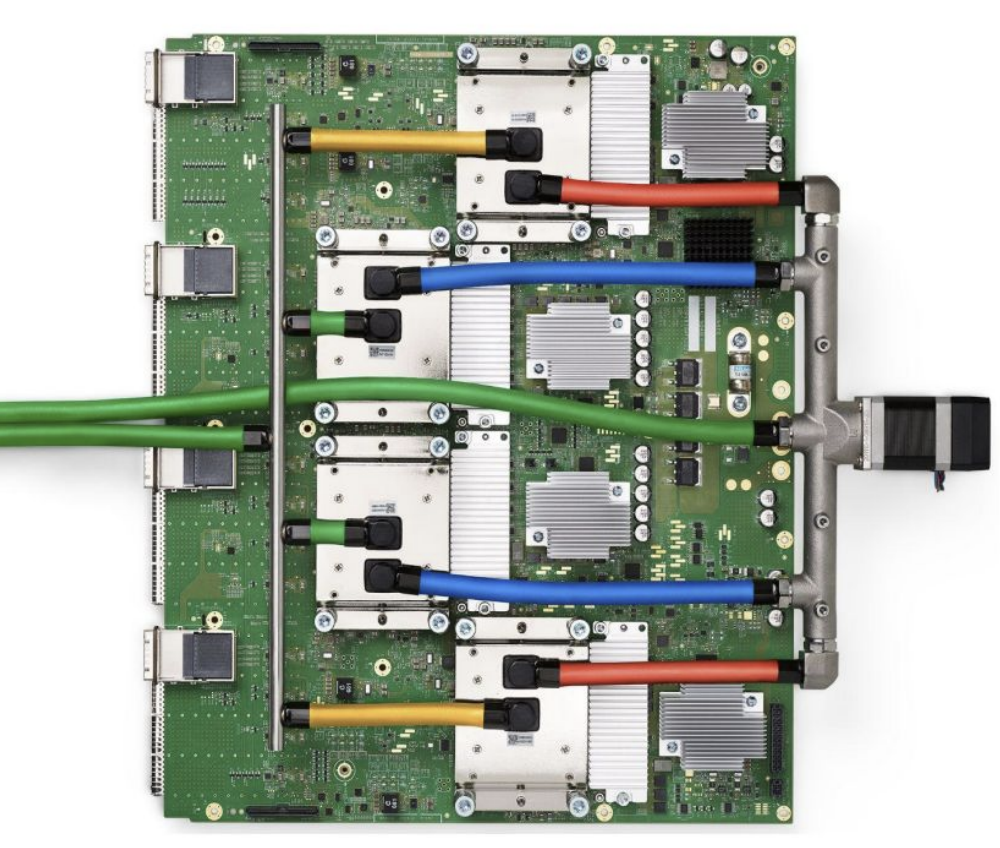
Here's an individual TPUv4 tray:
Note the image is simplified showing just one PCIe port, but actual trays have 4 PCIe ports (left side) — one per TPU.
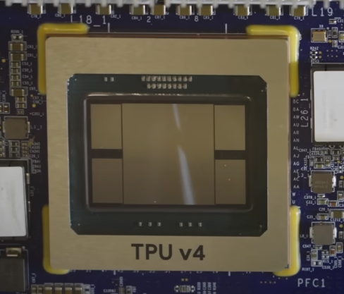
Here's an individual chip:
The central part is the ASIC; the 4 adjacent blocks are HBM stacks. The photo shows TPU v4, containing 2 TensorCore units internally, explaining the 4 HBM stacks.
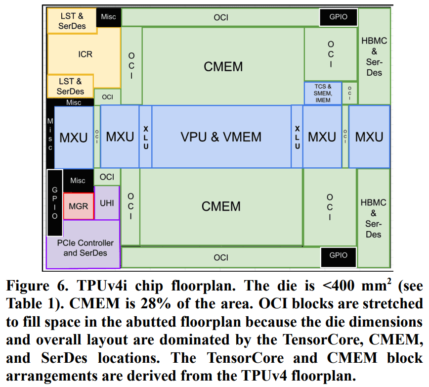
I couldn't locate TPUv4 chip schematics, so below is TPUv4i schematic; it resembles TPUv4 but has only one TensorCore since it's an inference chip:
Notice CMEM occupies substantial space in TPUv4i structure.
References
- [1] Google Blog: TPU Multi-Slice Training
- [2] Xu, et al. "GSPMD: General and Scalable Parallelization for ML Computation Graphs"
- [3] Jouppi et al. "Ten Lessons From Three Generations Shaped Google's TPUv4i"
- [4] How to Scale Your Model - TPUs
- [5] Domain Specific Architectures for AI Inference - TPUs
- [6] HotChips 2023: TPUv4
- [7] Google Cloud Docs: TPUv4
- [8] Jouppi et al. "In-Datacenter Performance Analysis of a Tensor Processing Unit"
- [9] Jouppi et al. "TPU v4"
- [10] PaLM training video
- [11] HotChips 2021: "Challenges in large scale training of Giant Transformers on Google TPU machines"
- [12] HotChips 2020: "Exploring Limits of ML Training on Google TPUs"
- [13] Google Blog: Ironwood
- [14] HotChips 2019: "Cloud TPU: Codesigning Architecture and Infrastructure"
- [15] ETH Zurich's Comp Arch Lecture 28: Systolic Array Architectures
- [16] Patterson presentation: "A Decade of Machine Learning Accelerators: Lessons Learned and Carbon Footprint"
- [17] Camara et al. "Twisted Torus Topologies for Enhanced Interconnection Networks"
- [18] Horowitz article: "Computing's Energy Problem (and what we can do about it)"
FAQ
What is this article about in one sentence?
This article explains the core idea in practical terms and focuses on what you can apply in real work.
Who is this article for?
It is written for engineers, technical leaders, and curious readers who want a clear, implementation-focused explanation.
What should I read next?
Use the related articles below to continue with closely connected topics and concrete examples.